Kontaktaufnahme

Live-Chat mit Tektronix-Vertretern. Verfügbar von 9 bis 17 Uhr CET Geschäftstage.

Anrufen

Kontaktieren Sie uns telefonisch unter

Verfügbar von 9 bis 17 Uhr CET Geschäftstage.

Download

Laden Sie Handbücher, Datenblätter, Software und vieles mehr herunter:

DOWNLOADTYP
MODELL ODER SCHLÜSSELWORT

Feedback

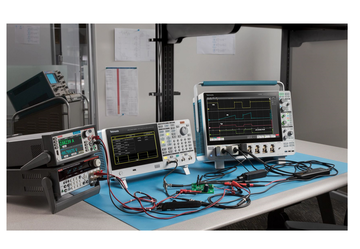
Wide Bandgap – Double Pulse Test Analysis

4/5/6 Series B MSO Option 4-WBG-DPT/5-WBG-DPT/6-WBG-DPT Application Datasheet

4/5/6 Series B MSO Option 4-WBG-DPT/5-WBG-DPT/6-WBG-DPT Application Datasheet

Semiconductor materials used in power electronics are transitioning from Silicon to Wide Bandgap (WBG) semiconductors such as Silicon Carbide (SiC) and Gallium Nitride (GaN) due to their superior performance at higher power levels in automotive and industrial applications. Due to its high operating voltage levels, SiC technology is finding applications in EV power trains, whereas GaN is primarily used in fast chargers for laptops, mobile devices, and other consumer devices.

Double Pulse Test (DPT) is an industry standard technique for measuring a range of important parameters during turn on, turn off, and reverse recovery.

In DPT, the DUT can either be the power device or a diode. The power device can be a Si, SiC, or GaN MOSFET or IGBTs.

The Wideband Gap Double Pulse Test application (Opt. WBG-DPT) on the 4/5B/6B Series MSO offers precise Wideband Gap measurements that make device and system validation easier. The application is compatible with all Tektronix VPI probes and, when used with the Tektronix IsoVu™ probes it helps uncover all the hidden artifacts of SiC or GaN devices at the circuit level.

The application offers automated measurements as per JEDEC and IEC standards. It offers unique features such as per-cycle analysis with annotation, flexibility with custom reference level settings, configurable integration points, and power preset that can be set based on the DUT designs.

The WBG-DPT application saves the designers time and cost. It’s quick to set up and measure, allowing design and test engineers to focus on debugging and improving target designs.

Key features and specifications

  • 18 double pulse test key measurements as per JEDEC and IEC standards
  • Ability to test SiC or GaN devices as well as Si MOSFET and IGBTs
  • Specify pulse regions such as the first, second, or multiple pulses of interest and correlate with the scalar results in the badge
  • Annotations on waveforms to show the regions of interest
  • Easily navigate the pulse region of interest for multi-pulse use case
  • Unique edge refinement algorithm to analyze noisy waveforms
  • Programmatic interface to all measurements and configurations enable the complete automation in test system applications
  • Support of Auto and Custom reference levels helps to precisely identify Start and Stop regions effectively
  • Hysteresis level configuration on the gate source helps to avoid false edges
  • Quickly add and configure measurements through the intuitive drag and drop interface on the 4/5/6 Series B MSO
  • Overlapped plot for Reverse Recovery (Trr) measurement
  • Added search directions (forward, backward) for effective debugging of pulse regions
  • Support for gate driver (AFG31000 Series) control for double pulse signal generation
  • Deskew feature for switching analysis

The application is designed based on the following standard references:

  • Double Pulse Test (DPT)
    • IEC 60747-9
    • JEP182
    • IEC 60747-8
  • Diode Reverse Recovery
    • JESD24-10
    • IEC 60747-9

Following measurements are performed:

  • Low side switching parameters and High side diode reverse recovery measurements
  • Low side and High side switching parameters

Test setup

The following schematic shows the measurement setup of the Double Pulse Test. This is an example of a half-bridge gate driver for a power MOSFET with both low and high side switching. On the high side, the source to gate pin is shorted to measure the diode reverse recovery current parameters.

The 4/5/6 Series B MSO are ideally suited for double pulse testing. Four channels are sufficient to test the high or low side switching separately, but if you would like to monitor the gate voltage as a source and diode reverse recovery parameters, then you may need more than four channels, in which case a oscilloscope with six or eight channels are ideal.

For DPT switching parameters, you need to acquire Vds, Id, and Vgs on the low side. Similarly, you need to check for Vgs on the high side when testing both high-side and low-side MOSFETs (refer Double Pulse test on the low and high side setup below). The diode reverse recovery is generally measured on High side, which needs Irr and Vrr. Tektronix recommends gate voltage as a qualifier source to avoid false detection of edges.

To accurately make the measurements on the high-side Vgs measurement, we need a measurement system that combines high bandwidth, high common mode voltage, and high common mode rejection. Along with its complete galvanic isolation, the Tektronix IsoVu system offers 1 GHz bandwidth, 2000 V common mode voltage, and 1 million to 1 (120 dB) common mode rejection ratio. It is a combination of these specifications that makes these kind of difficult measurements possible.

The IsoVu measurement system shows the details of what is occurring in the design and makes stable and repeatable measurements. The coupling due to parasitics between the switch node and the high and low-side MOSFETs are apparent, and the IsoVu measurement system has enough bandwidth to measure this dead time correctly.

WBG DPT EN US 61W 73888 4
Double Pulse test on the low and high side setup

WBG DPT EN US 61W 73888 4
Double Pulse test on the low side and Diode reverse recovery on the high side

AFG31000 as a gate driver

The Tektronix AFG31000 Series is a high-performance AFG with built-in arbitrary waveform generation, real-time waveform monitoring, and a large touchscreen. Providing advanced waveform generation and programming capabilities, waveform verification, and a modern touch-screen interface, the AFG31000 is an ideal choice of equipment that acts as a gate driver device. The AFG31000 includes the Double Pulse Test application, a downloadable plugin software application that enables double pulse applications for the power and semiconductor markets. The Double Pulse Test user interface provides touch-and-swipe or point-and-click control for generating at least two varying pulse widths. These pulses can be output to an isolated gate driver to trigger power devices such as MOSFETs or IGBTs and start conduction of current. The Double Pulse Test on the AFG31000 offers the design and test engineers the ability to generate voltage pulses with varying pulse widths on their DUTs. The design and test engineers are able to perform the Double Pulse Test in less than one minute, saving hours when compared to using a PC software or a microcontroller to perform the test with varying configurations.

The application also allows you to specify pulse regions of interest such as First pulse, Second pulse, and Multiple pulses. This input is used to validate and analyze the acquired waveforms on the oscilloscope and perform the WBG measurements.

Refer Application note on the AFG31000 for more details.

You can configure the AFG 31000 Series from the WBG-DPT application to generate a double pulse signal of required amplitude and pulse widths. The AFG output stimulus should be given to the gate driver of the power device to measure switching, timing, capacitance, and reverse recovery parameters of the device.

WBG DPT EN US 61W 73888 4

WBG DPT EN US 61W 73888 4

Power supplies

Based on the DUT requirements, a proper power supply must be chosen to power on the DUT. Designers can either use a DC power supply or a Source Measure Unit (SMU). The SMU is an instrument that can precisely source voltage or current and simultaneously measure voltage and/or current. It varies from a typical DC power supply in providing greater speed and precision, a wider operating range and better resolution, and built-in sweep capabilities.

Here are some of the recommended options for Tektronix power supplies that could be used for the Double Pulse Test.

  • High voltage power supply:
    • 2657 A High voltage Source Meter Unit (SMU)
    • 2260B-800-2, programmable DC power supply
  • Power supply to gate drive circuit:
    • 2230 or 2280S Series DC power supply

Probing and Accessories

When an engineer consider switching the designs from legacy silicon to WBG devices, some of the questions that arise are:

  • Is my test equipment capable of accurately measuring the fast switching dynamics exhibited by SiC devices?
  • How can I accurately optimize gate drive performance and deadtime?
  • Will common-mode transients affect the accuracy of measurements?
  • Is the observed ringing real or a result of probe response?

The traditional method for making a gate voltage measurement is by using a standard differential probe with MMCX connectors. This is important for gate voltage measurements on the high side. Measuring the gate voltage of a SiC power device is challenging since it is a low voltage signal (~20 Vpp) that is referenced to a node that may have a high DC offset and high dv/dt relative to the oscilloscope ground.

The Tektronix Isolated probes play a crucial role in making these floating gate measurements in a precise manner. The probe helps uncover the fast and floating signals that non-isolated probes are hiding. IsoVu™ Probe Technology virtually eliminates common mode interference using optical isolation. This delivers accurate differential measurements on reference voltages slewing ±60 kV at 100 V/ns or faster. With the IsoVu Generation 2 design, designers get all the benefits of IsoVu technology at 1/5 of the size.

The probes also offer versatile MMCX connectors and an unmatched combination of bandwidth, dynamic range, and common mode rejection to meet all the DPT test needs.

The best performance from the IsoVu measurement system is achieved when an industry standard MMCX connectors are inserted close to the test points. These connectors offer high signal fidelity and are recommended for precise and repeatable results. On the low side, use TPP with square pin to MMC adapter for Vgs probing, while on the high side, use TIVP with MMCX accessory.

Current probes

  • Current probes are required in the WBG setup to accurately make Id measurements. Tektronix offers a range of current probes to choose from.
  • TCP0030A is a high-performance, easy-to-use AC/DC current probe designed for use with and direct connection to oscilloscopes with the TekVPI™ probe interface. This AC/DC current measurement probe provides greater than 120 MHz of bandwidth with selectable 5 A and 30 A measurement ranges. It also provides exceptional low current measurement capability and accuracy to current levels as low as 1 mA, which is important for meeting the challenging current measurement needs.
  • For higher current needs, it's recommended to test with TCP0150 probes. In addition to the TCP family of probes, Tektronix offers the TRCP Series Rogowski current probes that are equipped with a BNC connector and work with any instrument supporting the BNC interface. Rogowski probes allow you to easily connect to large connection points such as bus bars or connect to small IC legs on a MOSFET or IGBT.

Here are the recommended probing details for DPT on Low side and diode reverse recovery setup on the High side:

  • Low side probing
    • Ch1: Vds - TPP or THDP Series voltage probe
    • Ch2: Vgs - TPP Series with MMCX adapter tips
    • Ch3: Id - TCP Series current probe
  • High side probing
    • Ch4: Irr - TCP - Series current probe
    • Ch5: Vds - THDP Series voltage probe

Here are the recommended probing details for DPT on Low side and High side:

  • Low side probing
    • Ch1: Vds - TPP or THDP Series voltage probe
    • Ch2: Vgs - TPP Series with MMCX adapter tips
    • Ch3: Id - TCP Series current probe
  • High Side Probing
    • Ch4: Vgs - TIVP Isolated probes with MMCX adapter tips
    • Ch5:Vds - THDP Series voltage probe

Measurements

Measurements offered by option WBG-DPT can be used to test power devices like MOSFET and IGBT as shown in the image below.

WBG DPT EN US 61W 73888 4

Power preset

The preset setting is useful to setup the oscilloscope for an optimal vertical scale, horizontal time base, sample rate, trigger source and level, and number of pulses for a specified Vds and Vgs levels.

WBG DPT EN US 61W 73888 4

Auto levels indicates the Start and Stop levels of the pulse regions as per JEDEC/IEC standards.

WBG DPT EN US 61W 73888 4

By default, the pulse region is defined as per the standard. For example, Eon in DPT is measured on the second pulse and Eoff is measured on the first pulse. However, you can configure the pulses as per your custom requirements. You can also choose the multiple pulse configuration to test more than two pulses. This offers greater flexibility based on the designs.

Generally, designers test with multiple pulses at different levels of drain current rather than making double pulse test. When switching the devices multiple times in continuous operation, this can stress the power devices and check for switching reliability.

WBG DPT EN US 61W 73888 4

During this operation, it is important to measure the turn on and turn off switching parameters of multiple edges. Multiple pulses are supported as part of the measurement configuration.

Since real world WBG waveforms are non-ideal and noisy in nature, you can define the sources by specifying custom start and stop levels in percentage units. This helps ease debug especially when Vds and Id are noisy and contain oscillations.

WBG DPT EN US 61W 73888 4

WBG Deskew

WBG DPT EN US 61W 73888 4

WBG Deskew calculates the skew between the Drain to Source Voltage (Vds) and Drain Current (Id) or Collector to Emitter Voltage (Vce) and Collector Current (Ic) when Power Device is MOSFET or IGBT respectively. The skew value is then applied on to the source to which Vds or Vce signal is configured on the oscilloscope.

WBG Deskew differs from the conventional scope-based Deskew operation. Conventionally, skew between probes is computed before starting any measurement on the test setup. In WBG-DPT, the skew of the measurement system is performed as a post-acquisition operation.

The Tektronix method of performing WBG deskew does not require any connection modification on the device. The deskew method models the Vds based on the acquired Id, Vgs, and circuit parameters (probe resistance, effective inductance). The mathematical modeled Vds is created and shown as Math. The acquired Vds signal and modeled Vds are overlapped to compute the skew and this skew is applied on the acquired Vds signal. This deskew procedure is simpler compared to conventional method.

Switching Parameter Analysis

WBG DPT EN US 61W 73888 4

Eon

Turn on energy for a MOSFET is measured as the integral of a power waveform computed from 10% of Id to 10% of Vds during turn on condition or specified levels.

Turn on energy for an IGBT is measured as the integral of a power waveform computed from 10% of Vge to 2% of Vce during turn on condition or specified levels.

WBG DPT EN US 61W 73888 4
Waveform during turn on time

WBG DPT EN US 61W 73888 4

Eoff

Turn off energy for a MOSFET is measured as the integral of power waveform computed between 10% of Vds and 10% of Id during turn off condition or specified levels.

Turn off energy for an IGBT is measured as the integral of a power waveform computed from 90% of Vge to 2% of Ic during turn off condition or specified levels.

WBG DPT EN US 61W 73888 4
Waveform during turn off time

WBG DPT EN US 61W 73888 4

Vpeak

Voltage peak is the maximum voltage peak value in the power device during turn off condition of collector current or drain current pulse. Usually, the voltage peak is measured in Eoff region.

Ipeak

Current peak is the maximum current peak value in the power device during turn on condition of a collector current or drain current pulse. Usually, the current peak is measured in Eon region.

Switching Timing Analysis

WBG DPT EN US 61W 73888 4

Td(on)

Turn on delay time for a MOSFET is the time interval between 10% of increasing Vgs to 90% of decreasing Vds during turn on condition or specified levels.

Turn on delay time for an IGBT is the time interval between 10% of increasing Vge to 10% of increasing Ic during turn on condition or specified levels.

Td(off)

Turn off delay time for a MOSFET is the time interval between 90% of the decreasing Vgs to 90% of increasing Vds during turn off condition or specified levels.

Turn off delay time for an IGBT is the time interval between 90% of the decreasing Vge to 90% of decreasing Ic during turn off condition or specified levels.

Tr

Rise time for a MOSFET is the time interval between 90% and 10% of the Vds during turn on condition or specified levels.

Rise time for an IGBT is the time interval between 10% and 90% of the Ic during turn on condition or specified levels.

Tf

Fall time for a MOSFET is the time interval between 10% and 90% of the Vds during turn off condition or specified levels.

Fall time for an IGBT is the time interval between 90% and 10% of the Ic during turn off condition or specified levels.

Ton

Turn on time is the sum of the turn on delay time and the rise time. It is the time interval between the rising of a voltage pulse across the input terminals which switches the power device from off-state to on-state.

Toff

Turn off time is the sum of the turn off delay time and the fall time. It is the time interval between the fall of a voltage pulse across the input terminals which switches the power device from on-state to off-state.

d/dt

Switching d/dt measures the rate of change of the voltage or current (slew rate), as it rises from the base reference level to the top reference level or as it falls from the top reference level to the base reference level.

WBG DPT EN US 61W 73888 4

Tdt

Dead time is the time delay between turn on time of the high side MOSFET and turn on time of the low side MOSFET during the simultaneous switching. It is the time interval between the configured falling edge level of one gate voltage and the configured rising edge level of another gate voltage. The default rising and falling edge levels are 50%.

Reverse Recovery Analysis

WBG DPT EN US 61W 73888 4

WBG DPT EN US 61W 73888 4
Diode reverse recovery area of a current

Trr

Reverse recovery time (Trr) is the time interval between the instant when the current passes through zero when changing from the forward direction to the reverse direction and the instant when extrapolated reverse current between A and B points reaches zero.

The Trr is comprised of two time intervals Ta and Tb when rectifiers respond with their own peak reverse recovery current Irr as shown in above figure. The Ta begins at the moment forward current has been ramped down and intersects the zero-current axis, and concludes at the rectifier Irr peak response point.

Reverse recovery current rise time (Ta)

Ta is defined as time taken by reverse recovery current to reach its maximum reverse peak value IRM.

Reverse recovery current fall time (Tb)

Tb is defined as time taken by reverse recovery current (or extrapolated current) to recovery back to zero from its reverse peak value. Hence, Trr = Ta + Tb.

Recovery Softness Factor (RSF)

RSF is defined as ratio of reverse recovery current fall time (Tb) to the reverse recovery current rise time (Ta).

Qrr

Reverse recovery charge (Qrr) is the total charge recovered from the power device during a specified integration time of a single collector current or drain current pulse, when the power device is switched from a specified forward current condition to a specified reverse voltage condition with forward biased gate condition.

The recovered charge is measured as:

WBG DPT EN US 61W 73888 4

Where:

t0 is the instant when the current passes through zero.

ti is the specified integration time, preferably when the current has reached 2% of Irr.

Err

The Reverse recovery energy (Err) is the energy dissipated within the power device during a specified integration time of a single collector current or drain current pulse, when the power device is switched from a specified forward current condition to a specified reverse voltage condition with forward biased gate condition.

The switching energy is the result of the integration of the product from the device voltage and current during the integration time ti.

WBG DPT EN US 61W 73888 4

Irrm

Reverse recovery current (Irrm) is the maximum reverse current that occurs during the reverse recovery time interval.

Diode d/dt

Diode d/dt measures the rate of change of voltage or current (slew rate) during the specified start and stop integration levels. Diode d/dt can be measured during rising or falling edge.

WBG DPT EN US 61W 73888 4
The image shows diode reverse recovery measurements with reverse recovery current and voltage captured on the high side

WBG DPT EN US 61W 73888 4
All measurements together, showing switching analysis, and timing parameters on the low side and diode reverse recovery measurements on the high side

WBG DPT EN US 61W 73888 4
The image shows overlapped plot on the Timing Reverse Recovery (Trr) measurement. The plot can be added from the measurement configuration.

Capacitance analysis

WBG DPT EN US 61W 73888 4

Qoss

Qoss measurement of a WBG-DPT application is the charge that must be supplied to the parasitic output capacitances of the power device during each switching cycle. This represents the output charge. The accurate measurement of output charge is of paramount importance as it directly affects switching speeds of a WBG device and capacitive property of SiC MOSFET body diode during turn on.

WBG DPT EN US 61W 73888 4

WBG DPT EN US 61W 73888 4

where,

t1 is the instance when the current passes through zero.

t2 is the specified time interval, preferably when Vds has reached 90% of the peak voltage.

WBG DPT EN US 61W 73888 4
Qoss measured on the diode current with annotations

Specification

Switching Parameter Analysis measurements panel

Measurement Description
Eon Measures the energy dissipated in the power device during turn on region using the configured levels.
EoffMeasures the energy dissipated in the power device during turn off region using the configured levels.
VpeakMeasures the peak voltage of the power device in the turn off region.
Ipeak Measures the peak current of the power device in the turn on region.

Switching Timing Analysis measurements panel

Measurement Description
Td(on) Measures the turn on delay time of the power device in the turn on region using the configured levels.
Td(off) Measures the turn off delay time of the power device in the turn off region using the configured levels.
Tr Measures the rise time of the power device in the turn on region using the configured levels.
TfMeasures the fall time of the power device in the turn off region using the configured levels.
TonMeasures the turn on time of the power device. It is the sum of the turn on delay time and the rise time.
ToffMeasures the turn off time of the power device. It is the sum of the turn off delay time and the fall time.
d/dtMeasures the rate of change of Drain to Source Voltage, or Drain Current between the specified levels.
TdtMeasures the time delay of the power device during simultaneous switching. It is the time interval between the falling edge of the first gate voltage and the rising edge of the second gate voltage.

Diode Recovery Analysis measurements panel

Measurement Description
Trr1Measures the reverse recovery time of the power device using the configured levels.
QrrMeasures the reverse recovery charge in the power device using the configured levels.
ErrMeasures the reverse recovery energy dissipated in the power device using the configured levels.
IrrmMeasures the reverse recovery current statistics.
Diode d/dtMeasures the rate of change of reverse recovery voltage or current between the specified levels.

Capacitance Analysis measurements panel

MeasurementDescription
QossMeasures the charge that must be supplied to the parasitic output capacitances of a power device during each switching cycle.
Plots
Waveform view with annotation, Recovery plot for Trr measurement.
Report
MHT and PDF formats, Data export to CSV format
Degauss/Deskew (static)
You can deskew voltage and current probes, degauss the current probes from the menus for each channel
WBG Deskew
Perform deskew between Vds and Id on the switching device2
Source support
Live analog signals, reference waveforms, and math waveforms
Pass/Fail
Test WBG-DPT measurements values against a specified limit and set actions for the instrument to take on failure2

Ordering information

Models and software licenses

ProductOptionsSupported instrumentsBandwidth available
New instrument purchase option4-WBG-DPT4 Series B MSO (MSO44B and MSO46B)
  • 200 MHz
  • 350 MHz
  • 500 MHz
  • 1 GHz
  • 1.5 GHz
Product upgrade optionSUP4-WBG-DPT
Floating licenseSUP4-WBG-DPT-FL
New instrument purchase option5-WBG-DPT5 Series B MSO (MSO54B, MSO56B, and MSO58B)
  • 350 MHz
  • 500 MHz
  • 1 GHz
  • 2 GHz
Product upgrade optionSUP5-WBG-DPT
Floating licenseSUP5-WBG-DPT-FL
New instrument purchase option6-WBG-DPT6 Series B MSO (MSO64B, MSO66B, and MSO68B)
  • 1 GHz
  • 2.5 GHz
  • 4 GHz
  • 6 GHz
  • 8 GHz
  • 10 GHz
Product upgrade optionSUP6-WBG-DPT
Floating licenseSUP6-WBG-DPT-FL

Software bundles

Supported instruments Bundle options Description
4 Series B MSO4-PRO-POWER-1Y1 Year License Pro Power Bundle
4-PRO-POWER-PERPerpetual License Pro Power Bundle
4-ULTIMATE-1Y1 Year License Ultimate Bundle
4-ULTIMATE-PERPerpetual License Ultimate Bundle
5 Series B MSO 5-PRO-POWER-1Y 1 Year License Pro Power Bundle
5-PRO-POWER-PER Perpetual License Pro Power Bundle
5-ULTIMATE-1Y 1 Year License Ultimate Bundle
5-ULTIMATE-PER Perpetual License Ultimate Bundle
5-PRO-AUTO-1Y 1 Year License Pro Automotive Bundle
5-PRO-AUTO-PERPerpetual License Pro Automotive Bundle
6 Series B MSO6-PRO-POWER-1Y1 Year License Pro Power Bundle
6-PRO-POWER-PERPerpetual License Pro Power Bundle
6-ULTIMATE-1Y 1 Year License Ultimate Bundle
6-ULTIMATE-PER Perpetual License Ultimate Bundle
6-PRO-AUTO-1Y 1 Year License Pro Automotive Bundle
6-PRO-AUTO-PER Perpetual License Pro Automotive Bundle

Recommended probes

Probe modelDescriptionQuantity
TCP0030A, TCP0150, or TRCP SeriesCurrent probe for making Ids measurement1
TIVP02, TIVP05, or TIVP1Voltage probe for making High-side Vgs measurement1
TPP0100, TPP0200, TPP0500B, or TPP1000Voltage probe for making Low-side Vgs measurement1
THDP0100, THDP0200, TMDP0200, TPP08503, or TPP10003Voltage probe for making Low-side Vds measurement1

Recommended function generators and power supply

Recommended function generators, gate driver source

ModelAnalog channelsFrequency rangePlug-in
AFG31000 Arbitrary Function Generator2425 MHz, 50 MHz, 100 MHz, 150 MHz, 250 MHzDouble Pulse Test Plug-In Application on the AFG31000

Recommended power supplies

ModelRated voltage rangesRated currentRated output power
2470 SMUMax 1000 VUp to 1 A20 W
2260B-800-20 - 800 V0 – 2.88 A720 W
2657AMax 3000 VMax 120 mA180 W