
Kontaktaufnahme
Live-Chat mit Tektronix-Vertretern. Verfügbar von 9 bis 17 Uhr CET Geschäftstage.
Anrufen
Kontaktieren Sie uns telefonisch unter
Verfügbar von 9 bis 17 Uhr CET Geschäftstage.
Download
Laden Sie Handbücher, Datenblätter, Software und vieles mehr herunter:
Feedback
BERTScope Clock Recovery Datasheet
BERTScope® CR Series Datasheet
Die Produkte dieses Datenblatts gehören nicht mehr zum Angebot von Tektronix.
Tektronix Encore nach aufgearbeiteten Testgeräten durchsuchen.
Garantie- und Supportstatus dieser Produkte überprüfen.
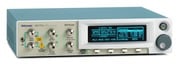
BERTScope® CR Series Datasheet
The BERTScope Clock Recovery CR Series advanced architecture measures and displays the PLL frequency response from 100 kHz to 12 MHz; the highest loop bandwidth available for jitter testing jitter testing on the market today. The first clock recovery instruments to allow full control of parameters including loop bandwidth, peaking/damping, and roll off.
Notice to EU customers
This product is not updated to comply with the RoHS 2 Directive 2011/65/EU and will not be shipped to the EU. Customers may be able to purchase products from inventory that were placed on the EU market prior to July 22, 2017 until supplies are depleted. Tektronix is committed to helping you with your solution needs. Please contact your local sales representative for further assistance or to determine if alternative product(s) are available. Tektronix will continue service to the end of worldwide support life.
Key performance specifications
- 150 Mb/s to 28.6 Gb/s with continuous data rate coverage to include Next-generation I/Os including PCIe 3.0, 10GBASE-KR, 16xFC, 25/28 G CEI, and 100GBASE-LR-4/100GBASE-ER-4
- Full and divided clock outputs with selectable divide ratios. Full-rate clock output up to 14.3 Gb/s, half-rate clock output from 14.3 Gb/s to 17.5 and 28.6 Gb/s
- Optional PCIe 2.5, 5, and 8 gb/s PLL loop analysis (Also requires jitter analysis option)
- CR175A and CR286A offer optional higher-sensitivity data inputs with clock recovery on signals as small as 40 mV amplitude (single ended), 20 mV amplitude (differential) – no DC-coupled data through path with this option
Key features
- Instrumentation quality clock recovery
- Accurate, variable loop bandwidth from 100 kHz to 12 MHz, with optional 24 MHz for the jitter transfer function (JTF) bandwidths of USB 3.0, SATA 6G, and PCIe Gen3
- Accurate, adjustable, self-measured, and displayed PLL loop bandwidth, peaking, and JTF – get the "Golden PLL" response needed for standards compliance testing
- Programmable peaking adjustment with first- and second-order roll-off capability
- USB control interface integrated into BERTScope view, or stand-alone with included BERTScope PC software
- DC-coupled data through path for accurate signal integrity
- Full and divided clock outputs with selectable divide ratios. Full-rate clock output up to 14.3 Gb/s
- Built-in equalizer function enables clock recovery under high ISI input conditions
- Data measurement capability
- Edge density measurement – determine the mark density of the signal under test
- Spread spectrum clock waveform view including dF/dt
- Ideal for spread spectrum clock (SSC) applications with large frequency excursions
- Optional direct spectral analysis of jitter components when under USB control from BERTScope or on PC using provided stand-alone software.
- Optional spectrum analyzer display with cursor measurements of jitter amplitude and frequency
- User-settable frequency-gated measurements for band-limited integrated jitter optionally available
- Preset band limits for PCI express Gen2 jitter spectrum
Applications
- Design/Verification of high-speed I/O components and systems
- Signal integrity analysis
- Certification testing of serial data streams for industry standards
The BERTScope CR series can be used with any sampling oscilloscope, BERT, or pattern generator.
Connecting the BERTScope CR clock recovery instrument to the BERTScope analyzer

Connecting the BERTScope CR clock recovery instrument to a sampling oscilloscope

Connecting the BERTScope CR clock recovery instrument to a BERT
Compliant clock recovery
Many communication standards now specify that jitter testing must be carried out using a reference clock that has been derived from the data signal. Typical Phase Lock Loop (PLL) characteristics are specified in terms of the -3 dB bandwidth of the recovery loop, the rate of rolloff of the frequency response, and the degree of response peaking allowable.
The BERTScope CR Series advanced architecture measures and displays the PLL frequency response from 100 kHz to 12 MHz; the highest loop bandwidth available for jitter testing on the market today. The first clock recovery instruments to allow full control of parameters including loop bandwidth, peaking/damping, and rolloff.
Design and test engineers can now find and lock onto signals of undefined or unknown data rate. The engineer can recover full-rate clocks, including spread spectrum clocks, for signals at data rates from 150 Mb/s to 12.5 Gb/s, and 14.2 Gb/s with extended data rate option. The engineer has full control of key parameters for variable loop bandwidth, peaking/damping and first- and second-order rolloffs, optimizing jitter tracking.

The BERTScope CR Series work seamlessly with BERTScope Analyzers - You can use the clock recovery instrument with the BERTScope by connecting the USB cable between the two instruments. The graphing capability can be displayed on the BERTScope analyzer by using the "To CR analysis" soft key.
Golden PLL
Many test standards require the use of a Golden PLL (Phase Lock Loop). Control of the BERTScope CR Series variable loop bandwidth allows for control of the jitter transferred to the recovered clock. When the loop bandwidth setting is narrow, much of the high-frequency jitter is removed from the clock signal. The narrowest LBW setting is desirable when a clock with the lowest possible jitter is required. When the loop bandwidth setting is wide, jitter is transferred to the recovered clock, emulating a clock signal similar to the CDR of the receiver under test. Each standard provides an optimum LBW setting for clock recovery often called the Golden PLL.
Recover Spread Spectrum clocks for testing to electrical serial bus standards
Spread Spectrum Clocking (SSC) is an increasingly required feature of serial bus standards. When employed, it can prove difficult to track but its effect must be included in test. These instruments are able to track SSC correctly with large frequency excursions up to 5000 ppm, making them unique amongst clock recovery test solutions. The BERTScope CR series is the first clock recovery instrument to recover clocks from spread spectrum clocked signals used in Serial ATA, SAS, PCI Express, and USB applications.


Spread spectrum clocks exhibit low-frequency (30-33 kHz) modulation, for example, resulting in 225 UI (Unit Interval) deviation when imposed on a 3 Gb/s data signal. This frequency deviation is tracked accurately by the clock recovery instrument when the optional 5-piece cable set is used with the BERTScope CR Series and BERTScope Analyzer. This cable set is matched to compensate for the 5 ns delay in BERTScope Analyzer with SSC signals, thus avoiding jitter amplification.
A signal with SSC was measured with the BERTScope CR Series. Outputs on the rear panel of the instrument provide monitoring points to view the loop behavior. When viewed on a low-bandwidth, real-time oscilloscope, the triangular waveform characteristic of SSC is visible in the lower trace. The upper waveform displays the difference in phase between data input and clock recovery output.
View and measure SCC modulation
The BERTScope CR Series instruments also allow you to view and measure SSC generated in your system. Problems with the SSC modulation waveform can result in clock rate deviation beyond the capability of the channel or receiver. Excessively fast transitions often cause bit errors, as the receiver CDR cannot track the fast change. Conversely, modulation with long periods of no clock rate change cause energy peaks in parts of the spectrum, resulting in EMI (Electro-Magnetic Interference) which SSC is supposed to reduce.

Excessive noise in the SSC modulator can cause tracking problems in the receiver CDR, resulting in bit errors.

Cleaner SSC modulation
The SSC Waveform view provides a calibrated plot of the SSC modulation, allowing the user to instantly see if any of these modulation problems exist. The vertical axis represents the carrier deviation, and can be scaled in units of either frequency deviation (PPM) or time (ps).

A revealing dF/dT waveform showing poor performance
To avoid the tracking and possible EMI problems from incorrect deviation rates, some of the new serial data standards are specifying the minimum and maximum rate of change of the SSC carrier frequency. The BERTScope CR Series can directly display the dF/dt function, and provide a parametric measurement of the minimum and maximum peaks.
User interface
The instruments can be used with the BERTScope or in stand-alone operation. Inexperienced users and experts alike will respond to the same ease and accuracy already available in the BERTScope Analyzer. Perfect companions to the BERTScope, the clock recovery instruments smoothly integrate with the analyzer, seamlessly sharing a common user interface. A single USB connection and supplied high-quality microwave coaxile cables connect the two units together - that is all that is required to start measurements. The BERTScope automatically senses the presence of the clock recovery instrument, and control is achieved through the Clock Recovery setup screen. It is that simple. The same information is also immediately available on the front-panel display, showing parameters such as the PLL bandwidth, lock status, bit rate, peaking, and rolloff. The system is designed to make sure that you are always aware of the test conditions, always aware of the factors in play that will affect your measurement results.
Graphing capability on the BERTScope Analyzer allows users to plot loop response and inverse response curves for the settings in use. The -3 dB point and peaking values are also measured and clearly displayed.
For engineers wanting to use test equipment already available on their lab bench, the same control views are available on a PC running the BERTScope PC stand-alone software, included with the product. Interface to the PC is through a standard USB port. The instrument can be controlled directly through the front-panel display and knob. In keeping with the BERTScope philosophy of being the easiest-to-use signal integrity tools available, the clock recovery instruments provide the information you most need, right up front. For easy verification of compliance, the correct characteristics are automatically set when a given standard is selected from a pull-down menu. However, for users wanting to explore the limits of their designs, full control of parameters is also easily available. A good example of this is for systems where restricting the buildup of jitter is critical. Clock recovery plays a crucial role in this, and the ability to emulate a clock recovery source with excessive peaking is a great way of understanding the system sensitivity to jitter gain. Each instrument has variable jitter peaking that goes way beyond simple compliance, and allows jitter gain in excess of 10 dB if desired.
Remote control of the instrument is easily accessible by USB through the BERTScope Analyzer. TCP/IP and GPIB protocol interfaces are supported by USB and the software developers kit.
Importance of data and recovered clock path delay matching
When recovering a clock with SSC modulation or containing a large amount of periodic jitter, it is important to precisely match the delay path of the data signal and recovered clock between the BERTScope CR Series and the test instrument. The data path must have additional delay added corresponding to the trigger latency between the clock edge at the instrument clock or trigger input, and the instant when the instrument actually samples the data. Without matching, at high data rates this delay can be several hundred or even thousand unit intervals. This could have the apparent effect of reduced eye timing margin in masks, higher bit error rates, and inflated jitter measurements.

Clock Recovery Loop Bandwidth versus Data Rate - The BERTScope CR Series has a variable loop bandwidth from 100 kHz to 12 MHz. The loop bandwidth is calibrated when operating within the range shown in green in the plot to the left.
When the BERTScope CR Series is used with a BERTScope Analyzer, this problem is eliminated by using the precision Matched Cable Set. The set is composed of high-quality low-loss cables, which are carefully matched for differential phase and delay for use with the BERTScope. The set consists of five cables: a pair of phase-matched cables for CR data input, a pair of phase- and delay-matched cables for the data signal between the CR and BERTScope error detector inputs, and a delay-matched cable for connecting the CR clock output to the BERTScope clock input.

Optional 5-piece matched cable set
Jitter spectrum display
The BERTScope CR Series options 12GJ, 17GJ, and 28GJ feature all of the clock recovery capability and performance of the BERTScope CR Series, with the addition of a powerful jitter measurement and analysis tool - Jitter Spectrum. The Jitter Spectrum view is a plot of jitter magnitude versus frequency. The Jitter Spectrum is a powerful tool for quantifying and isolating the source of jitter components in the device under test. Frequency peaks from unrelated clocks, switching power supplies, and other periodic jitter that is uncorrelated with the data clearly show up in the "spectrum analyzer" type display. The vertical axis is scaled in either % of UI or time. Either linear or log scaling can be selected.

Jitter spectrum display.
Frequency-gated measurement
Because the clock recovery process tracks the lower-frequency components in a serial data receiver, the system is generally less sensitive to low-frequency jitter components than to the higher-frequency ones. This varying sensitivity to different frequency components is factored into the compliance tests of various serial data standards, such as second-generation PCI Express. Thus, the ability to measure the magnitude of the jitter components emitted from a transmitter in various frequency bands is important for system validation. The BERTScope CR Series features a band-selected integrated jitter measurement. The user enters the lower and upper limits of the frequency band which the jitter measurement is to be integrated over. A real-time display provides the total integrated jitter within this band. Up to three different simultaneous frequency bands can be entered in the instrument.

Frequency-gated measurement
Help isolating jitter sources
Periodic jitter components uncorrelated to the data are often caused by coupling of system clocks, crosstalk from uncorrelated data lines, power-supply ripple pattern dependent jitter, etc. These show up as sharp frequency peaks in the jitter display. Cursor measurements allow the user to quickly find the frequency associated with the suspect peak.
Duty cycle dependent jitter measurement
Jitter components can often be related to the data pattern. Duty Cycle Dependent Jitter (DCD) occurs when consecutive bits in the data pattern have unequal lengths. The unequal lengths can be either due to ones and zeros having different durations or due to the use of sub-rate clocks. For example, a half-rate clock would use a delayed version of its rising edge to clock the second of two consecutive bits. If the delay is different from the nominal unit interval (bit length) then every two bits become a sequence of a long bit followed by a short bit. The BERTScope CR Series can directly measure the DCD in the incoming data stream and report the result in percentage of the unit interval (UI) on the front-panel display.

DCD data pattern

CD jitter measurement
Powerful tools to analyzer jitter
Measurement of the total jitter in a serial data signal provides useful information to predict the accuracy of the system. However, a total jitter number does not provide very much information on the nature of the jitter. This information is necessary to determine the susceptibility of the receiver to various jitter components, and is useful to identify the source. The BERTScope CR Series clock recovery instrument provides powerful jitter analysis capability.
Compliant clock recovery for 100 Gb Ethernet and OIF-CEI 28G
The BERTScope CR286A is designed to support emerging high-speed standards such as 100 Gb Ethernet (100 GbE), which operates at a line rate of 25.78125 Gb/s. The CR286A goes a step further with a maximum data rate of 28.6 Gb/s to support OIF-CEI 28G. These instruments have all the core features of the CR125A, the award-winning BERTScope clock recovery product, with extended locking range to 26 and 28.6 Gb/s.

BERTScope CR series high-sensitivity model for low-amplitude signals
The CR286A with Option HS includes the same features as the CR models, but with higher input sensitivity for applications involving small signals down to 40 mV (single ended) or 20 mV (differential). This is achieved by removing the power tap-offs from the instrument, allowing the user to access the full sensitivity range. The HS option is ideal for optical applications, where small amplitude signals are common, or for electrical test setups where the extra sensitivity is critical. It offers total control over what fraction of the signal should be dedicated to clock recovery.
Recover clocks under closed eye signal conditions
The BERTScope CR family has built-in equalization, so engineers can recover a clock even when the data input signal suffers ISI from frequency-dependent loss conditions that close the eye completely.

The BERTScope CR Series can recover a clock under harsh conditions such as a 10 Gb/s PRBS-31 data pattern with 71" of trace on the ISI board - a capability that becomes even more important at 25.78 Gb/s.
At high bit rates such as the 100 GbE rate of 25.78125 Gb/s, inter-symbol interference that was a problem at 10 Gb/s can pose an even greater threat, turning a partially open eye into one that is completely closed. With built-in linear equalization, you can rely on the BERTScope CR Series to recover a clock while adhering to the loop bandwidth and peaking conditions you have set. This makes triggering a downstream instrument such as a BERTScope or Tektronix oscilloscope easy, while remaining compliant with the Golden PLL requirements in the high-speed standard of interest. The data signal through path is unaffected by the clock recovery equalization.

Gain versus equalizer setting
This graph shows approximate equalizer gain in dB versus the equalizer setting in the CR at 15 and 25 Gb/s input data rate. For the highest equalizer setting at 25 Gb/s input data rate, more than 20 dB of linear equalization is applied to the input, enabling clock recovery on signals that would normally not achieve successful lock. The equalizer operates over the full data rate range of the CR.
Specifications
All specifications are guaranteed unless noted otherwise. All specifications apply to all models unless noted otherwise.
- Key specifications
-
- Data inputs/outputs
-
Characteristic CR125A CR175A CR286A CR286A Option HS Input sensitivity 100 mV single ended (typical) 50 mV differential (typical) 40 mV single ended (typical) 20 mV differential (typical) Input data rate coverage 150 Mb/s to 12.5 Gb/s 150 Mb/s to 17.5 Gb/s 150 Mb/s to 28.6 Gb/s 150 Mb/s to 28.6 Gb/s Data insertion loss 2 dB (min), 2.6 dB (typical), 3 dB (max), up to 12.5 Gb/s 1 - Data input voltage range -5 V (min), +5 V (max) -5 V (min), +5 V (max), 1 Vp-p (max) Measured edge density accuracy ±1%, up to 14.3 Gb/s, ±3% >14.3 Gb/s Equalization range 0 to 10 dB Data output Up to 12.5 Gb/s 1 - - Clock and subrate clock outputs
-
Characteristic CR125A CR175A CR286A CR286A Option HS Loop bandwidth 100 kHz to 12 MHz 200 kHz to 12 MHz above 14.3 GHz - up to 24 MHz with Option XLBW ext. loop BW Peaking 0-6 dB, 500 kHz - 12 MHz 0-5 dB, 12 MHz - 24 MHz with Option XLBW Intrinsic jitter (typical) 250 fs Clock output range Full-rate clock for input data rates to 14.3 Gb/s Half-rate clock for input data rates >14.3 Gb/s Sub-rate divider ratios For input data rate to 14.3 Gb/s: Full rate divided by 1, 2, 4, 5, 6, 7, 8, 9, 10, 12, 14, 16, 18, 20, 24, 25, 28, 30, 32, 35, 36, 40, 42, 45, 48, 49, 50, 54, 56, 60, 63, 64, 70, 72, 80, 81, 90, 100, 108, 112, 120, 126, 128, 140, 144, 160, 162, 168, 180, 192, 196, 200, 216, 224, 240, 252, 256, 280, 288, 320, 324, 336, 360, 384, 392, 432, 448, 504, 512, 576, 648 For input data rate >14.3 Gb/s: Full rate divided by 2, 4, 8, 10, 12, 14, 16, 18, 20, 24, 28, 32, 36, 40, 48, 50, 56, 60, 64, 70, 72, 80, 84, 90, 96, 98, 100, 108, 112, 120, 126, 128, 140, 144, 160, 162, 180, 200, 216, 224, 240, 252, 256, 280, 288, 320, 324, 336, 360, 384, 392, 400, 432, 448, 480, 504, 512, 560, 576, 640, 648, 672, 720, 768, 784, 864, 896, 1008, 1024, 1152, 1296
1Data through path only recommended for use below 12.5 Gb/s. Use external pick-off tees and terminate output connector above 12.5 Gb/s.
Instrument characteristics
- Data interfaces
- 50 Ω differential or single-ended, DC coupled. APC 3.5 user-replaceable Planar Crown® adapter
- Data rate coverage
- 150 Mb/s to 28.6 Gb/s (12.5 Gb/s for CR125A, 17.5 Gb/s for CR175A)
- Data insertion loss
- 2 dB (min), 2.6 dB (typical), 3 dB (max) from data input to data output
- Data input voltage range
- –5 v (min), +5 v (max)
- Input sensitivity
- 100 mV single ended (typical)
50 mV differential (typical)
- Measured edge density resolution
- ±1%
- Measured phase deviation
- Displayed as % RMS and % peak-peak, 10-90% peak-peak available range
Clock outputs
- Clock interfaces
- 50 Ω single-ended, AC coupled. APC 3.5 user-replaceable Planar Crown® adapter
- Clock output range
- 150 MHz to 12.5 GHz (full-rate clock output)
- Loop bandwidth
- 100 kHz - 12 MHz variable
- Loop bandwidth accuracy
- ±10% (1100 pattern)
- Locking range
- 50 MHz default, adjustable to 10-500 MHz
- Peaking
- 0-6 dB from 500 kHz - 12 MHz, 0 dB from 100 kHz - 500 kHz
- Peaking accuracy
- Greater of ±10% of setting, or 0.5 dB
- Frequency response
- –20 dB/decade to –40 dB/decade
- Intrinsic jitter
- Measured at 800 mVp-p input amplitude, 10 gb/s, 1010 pattern, 2 MHz loop bandwidth setting, and 0.5 dB peaking
- Typical
- 70 fs
- Maximum
- 250 fsrms
- Output frequency deviation tracking range
- +500/-5500 ppm (+0.05/-0.55%)
(Tracking 30-33 kHz triangle modulated SSC)
- Minimum input return loss
- 15 dB
- Output waveform Rise/Fall times (20/80%)
- 25 ps (typical), 30 ps (max)
- Output amplitude
- 250 mV (min)
900 mV (max) at clock rates ≤12.5 gb/s
700 mV (max) at clock rates >12.5 gb/s
- Output amplitude setting accuracy
- Greater of 10% or 30 mV, >50 MHz clock output frequency
Subrate clock output
(as specified for clock output except for the following)
- Sub-rate divider ratios
- Full rate divided by 1, 2, 4, 5, 6, 7, 8, 9, 10, 12, 14, 16, 18, 20, 24, 25, 28, 30, 32, 35, 36, 40, 42, 45, 48, 49, 50, 54, 56, 60, 63, 64, 70, 72, 80, 81, 84, 90, 96, 98, 100, 108, 112, 120, 126, 128, 140, 144, 160, 162, 168, 180, 192, 196, 200, 216, 224, 240, 252, 256, 280, 288, 320, 324, 336, 360, 384, 392, 432, 448, 504, 512, 576, 648
Trigger output (Rear panel)
- Interface type
- SMA, 50 Ω, DC coupled
- Latency
- 300 ms
Trigger input (Rear panel)
- Interface type
- SMA, 50 Ω, DC-coupled to 0 V
- Threshold
- 1.5 V
- Minimum pulse width
- 50 ns
Control
- Control interface
- USB cable (supplied). unit also provides hub capability giving 3 additional USB ports
- Device information
- Serial number, revision codes available using front-panel display
Jitter spectrum
- The performance of the BERTScope CR Series Option GJ Jitter Spectrum and DCD measurements are listed in the specifications below. The performance of the clock recovery functionality remains identical as listed in the BERTScope CR Series specifications.
- Minimum frequency
- 200 Hz
- Maximum frequency
- 90 MHz
- Minimum frequency resolution
- 200 Hz
- Maximum jitter
- Limited only by the ability of the clock recovery to lock with PLL BW at 0.5 MHz and 0.5 dB peaking
- Vertical units
- % UI or ps
- Vertical scale
- Log or linear
- Frequency scale
- Log or linear
- Maximum number of integrated measurement frequency bands
- 3
Duty cycle dependent jitter
- Units
- % UI or ps
- Maximum range
- 50% UI
Physical
- Height
- 92.25 mm (3.75 in.)
- Width
- 393.7 mm (15.5 in.)
- Depth
- 336.5 mm (13.25 in.)
- Weight
- 9.07 kg (20 lbs)
Environmental
- Temperature
-
- Operating
- 0 °C to 35 °C ( 32 °F to 95 °F)
- Nonoperating
- -18 °C to 60 °C ( -0.4 °F to 140 °F)
- Relative humidity
-
- Operating
- 20-80% at or below 35 °C (95 °F)
- Nonoperating
- 5-90% at or below 60 °C (140 °F)
- Vibration (5-500 Hz)
-
- Operating
- 0.2 grms
- Nonoperating
- 2.09 grms
Ordering information
Clock recovery instruments
- CR125A
- 12.5 Gb/s Clock Recovery Instrument
- CR175A
- 5 Gb/s Clock Recovery Instrument
- CR286A
- 28.6 Gb/s Clock Recovery Instrument
Options
Clock recovery options
| Option | Description | CR125A | CR175A | CR286A |
|---|---|---|---|---|
| PCIE | PCIe PLL analysis (requires 12GJ, operates at 2.5 G and 5 G only) | X | X | X |
| PCIE8G | PCIe PLL analysis (requires 12GJ, operates at 2.5 G, 5 G and 8 G ) | X | X | X |
| HS | Add High-sensitivity Clock Recovery (This option has no data outputs. 1) | X | ||
| XLBW | Add Extended Loop Bandwidth in the clock recovery | X | X | X |
| 12GJ | Add Jitter Spectrum Analysis from 1.2 to 11.2 Gb/s | X | ||
| 17GJ | Add Jitter Spectrum Analysis from 1.2 to 11.2 Gb/s | X | ||
| 28GJ | Add Jitter Spectrum Analysis from 1.2 to 11.2 Gb/s | X | ||
| CA1 | Single Calibration or Functional Verification | X | X | X |
| C3 | Calibration Service 3 Years | X | X | X |
| R3 | Repair Service 3 Years (including warranty) | X | X | X |
| -R3DW | Repair Service Coverage 3 Years (includes product warranty period); 3-year period starts at time of customer instrument purchase | X | X | X |
1This option removes the data output connectors. If data outputs are necessary for the application, use external components to split the signal before applying the signal to the CR inputs.
Recommended accessories
Accessories
- CR125ACBL
- High-performance Delay-matched Cable Set (required for BERTScope and CRU in SSC applications)
- 100PSRTFILTER
- 100 ps rise time filter
- BSA12500ISI
- Differential ISI board
- PMCABLE1M
- Precision phase-matched cable pair, 1 m
- SMAPOWERDIV
- SMA power dividers
- BSASATATEE
- BSA-SATA-Tee for OOB signaling
- SATATESTSW
- Serial ATA interop test suite automation software
- BSARACK
- BSA rackmount kits

Tektronix is registered to ISO 9001 and ISO 14001 by SRI Quality System Registrar. 65W-25479-9
