
Kontaktaufnahme
Live-Chat mit Tektronix-Vertretern. Verfügbar von 9 bis 17 Uhr CET Geschäftstage.
Anrufen
Kontaktieren Sie uns telefonisch unter
Verfügbar von 9 bis 17 Uhr CET Geschäftstage.
Download
Laden Sie Handbücher, Datenblätter, Software und vieles mehr herunter:
Feedback
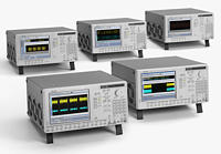
Arbitrary Waveform Generator
AWG7102 • AWG7101 • AWG7052 • AWG7051
Die Produkte dieses Datenblatts gehören nicht mehr zum Angebot von Tektronix.
Tektronix Encore nach aufgearbeiteten Testgeräten durchsuchen.
Garantie- und Supportstatus dieser Produkte überprüfen.
AWG7102 • AWG7101 • AWG7052 • AWG7051
Features & Benefits
- 10 GS/s (20 GS/s) and 5 GS/s Models
- 1 or 2 Arbitrary Waveform Outputs
- Accurate Timing with only 20 psp-p Total Jitter (at 10-12 BER, Typical)
- 45 ps Tr/Tf (20% to 80%)
- ±100 ps Range (1 ps Resolution) Interchannel Skew Control
- 2 or 4 Variable-level Marker Outputs
- Accurate Timing with only 30 psp-p Total Jitter (at 10-12 BER, Typical)
- 45 ps Tr/Tf (20% to 80%)
- Up to 300 ps Range (1 ps Resolution) Delay Control
- Vertical Resolution up to 10 bit Available: 10 bits (No Marker Output) or 8 bits (with Two Marker Outputs)
- Up to 64 M (64,800,000) Point Record Length Provides Longer Data Streams
- Down to 100 fs Resolution Edge Timing Shift Control
- Sequencing Creates Infinite Waveform Loops, Jumps, and Conditional Branches
- Real-time Sequencing Creates Infinite Waveform Loops, Jumps, and Conditional Branches
- Intuitive User Interface Shortens Test Time
- Integrated PC Supports Network Integration and Provides a Built-in DVD, Removable Hard Drive, LAN, and USB Ports
Applications
- Disk Drive (Magnetic/Optical) Read/Write:
- Up to 5 Gb/s Data Rate (2 Points/Cell) or 50 ps Timing Resolution
- Telecom/Data Communications:
- Up to 10 Gb/s Data Rate (Binary, Pre/De-emphasis, and Multilevel Logic)
- Wireless Communications:
- Up to 5 GHz (4 Waveform Points/Cycle) Arbitrary RF/IF and Wide-bandwidth Modulation I and Q Baseband Signals
- Mixed-signal Design and Test:
- 2-channel Analog plus 4-channel Marker Outputs
- High-speed, Low-jitter Data/Pulse and Clock Source
- Real-world, Ideal, or Distorted Signal Generation – Including All the Glitches, Anomalies, and Impairments
- Enhanced/Corrupted Playback of DSO Captured Signals
- Waveform Vectors Imported from Third-party Tools such as MATLAB, MathCAD, Excel, and Others
The AWG7000 Series of Arbitrary Waveform Generators Delivers the Industry’s Best Mixed-signal Stimulus Solution for Ever-increasing Measurement Challenges
The AWG7000 Series Arbitrary Waveform Generator delivers a unique combination of superior signal stimulus, unrivaled sample rate, bandwidth and signal fidelity, and uncompromised usability.
This family offers the industry’s best solution to the challenging signal stimulus issues faced by designers verifying, characterizing, and debugging sophisticated electronic designs.
With sample rates from 5 GS/s to 20 GS/s (10 bits), together with 1 to 2 output channels, the toughest measurement challenges in the disk drive, communications, digital consumer, and semiconductor design/test industries can be easily solved.
The open Windows (Windows XP)-based instruments deliver ease of use and allow connectivity with peripherals and compatibility with third-party software.
Application Examples
The need for performance arbitrary waveform generation is broad and spans over a wide array of applications. With the AWG7000 Series, Tektronix’ 3rd generation of industry-leading Arbitrary Waveform Generators represent a new benchmark in performance, sample rate, signal fidelity, and timing resolution.
The ability to create, generate, or replicate either ideal, distorted, or “real-life” signals is essential in the design and testing process. Signal generation with controllable rise and fall times, noise or jitter; pre-emphasis, multilevel, and mixed signals; wideband RF, and fast-changing signals are just some of the capabilities of the AWG7000 Series.
Pre/De-Emphasized Signal Generation
Figure 1: 5 Gb/s Pre/De-emphasized signal.
With increasing transmission speeds and to compensate for frequency characteristics of “lossy” media, the technique of pre/de-emphasis is increasingly applied. Serial data standards such as PCI Express and others have also included pre/de-emphasis tests as a requirement to meet the respective compliance test specification.
The basic theory of pre-emphasis is that for any series of bits of the same value, the first bit always has a higher voltage level than the following bits. By doing so, frequency characteristics of transmission lines can be compensated thus the signal fidelity at the receiver side increased.
The AWG7000 Series, with its performance and analog output, enables users to directly generate pre/de-emphasized signals for next-generation serial data standards. It also enables users to generate 3-level signals as required for SATA Out-of-Band (OOB) testing.
The direct generation of such signals provides an increased signal quality and avoids cumbersome signal generation using multiple channels and a power combiner. See Figure 1.
Multilevel Signal Generation

Figure 2: 20 Gb/s 4PAM signal (5 GS/s; AWG7101).
The requirements for serial interfaces are continuously increasing. Higher and higher data rates are required, and the performance of cables and circuits is moving closer to their theoretical limits. One technique to increase the data rate without increasing the transition rate is by applying multilevel signals, wherein a signal can assume more than the standard binary 2 levels.
In multilevel signaling one can think of multilevel discrete amplitudes of a signal. This phenomenon is known as Pulse Amplitude Modulation or PAM. A 4PAM signal, a signal with 4 different amplitudes, increases the data rate by four without increasing the transition rate of the signal. Multilevel signals are not only applied for data transmission. Multilevel memory chips, storing more than a single bit in an individual memory element, are being produced and multilevel coding of data for storage on optical disks is being considered as an efficient way to increase storage capacity.
The AWG7000 Series enables you to test your latest design by generating any kind of mixed or multilevel signal. See Figure 2.
Signal Generation for Storage Device Testing

Figure 3: Hard disk read channel signal (5 Gb/s 2 points per cell); AWG7101 with 10 GS/s.
Increasing capacity requirements for storage devices leads to the development of new and faster read-and-write strategies for magnetic as well as optical storage devices. Multilevel coding of data for storage on optical disks is also being considered as an efficient way to increase storage capacity.
The AWG7000 Series, with its ability to generate an accurate reproduction of the readandwrite signals, enables users to design, develop, and test the latest storage devices. With sample rates up to 20 GS/s, and the generation of up to 6 signals (2 analog plus 4 marker) with a clock timing resolution of 100 ps, the AWG7000 Series represents a new benchmark in the industry. See Figure 3.
Wideband RF-signal Generation

Figure 4: UWB (MBOA) three band (480 Mb/s 1795 MAC bytes 96 symbol payload); 3.168 GHz-4.752 GHz; AWG7102; Interleave at 15.84 GS/s; 0.5 Vp-p.
In the RF world, technologies ranging from a wireless mouse to a satellite image require test equipment that can provide enough sample rate and resolution to recreate even the most complex RF behavior. The latest digital RF technologies often exceed the capabilities of current test equipment to generate wide-bandwidth and fast-changing signals that are increasingly seen in many wireless applications such as radar, UWB, and others.
The AWG7000 Series enables the direct generation of RF signals and their output through the D/A converter for signals up to a carrier frequency of 5 GHz and a bandwidth of 5.8 GHz. The direct generation of IF or RF signals avoids I/Q degradations and lengthy adjustments associated with traditional generation using I/Q modulators. The AWG7000 Series with its maximum sample rate of 20 GS/s is the sole solution that allows a direct RF signal generation for up to 5 GHz. See Figure 4.
Additional Software Application Tools Extending Waveform Generation

RFXpress (RFX100)
RFXpress is a software package that synthesizes digitally modulated baseband, IF, and RF signals. It takes IQ, IF, and RF signal generation to the next level and fully exploits the wideband signal generation capabilities of Arbitrary Waveform Generators (AWGs). Supporting a wide range of modulations, as well as the symbol map functions, the software allows you to define your own modulation.
UWB-WiMedia signal creation, a software module for RFXpress, has the capability to digitally synthesize and generate RF signals in Band Groups 1 and 2 of the UWB spectrum. As per the latest WiMedia specification, signals will band hop in real-time over 1.5 GHz modulation bandwidth including all the different preamble synchronization sequences, cover sequences, TFCs, and band groups. All six band groups (BG1 to BG6) can be generated with band hopping in either IQ or IF. The conformance mode enables you to generate all signals that conform to WiMedia’s specifications, while the custom mode allows you to adjust the signals for stress and margin testing.

SerialXpress® (SDX100)
SerialXpress enables creation of exact waveforms required for thorough and repeatable design validation, margin/characterization, and conformance testing of high-speed serial data receivers. It considerably simplifies the signal creation and Jitter simulations, thus reducing overall development and test time. In addition to supporting generation of Jitter (Random, Periodic (sinusoidal), ISI, and DCD) SerialXpress also supports SSC, pre-emphasis, and noise addition. This allows the user to create a combination of various impairments simultaneously to stress the receiver.
Both RFXpress and SerialXpress are powerful easy-to-use software packages to synthesize RF and high-speed serial data signals respectively for arbitrary waveform generators (AWG). It runs as an integral part of the AWG7000 Series arbitrary waveform generators or from an external PC.
Characteristics
Arbitrary Waveforms
Characteristic | AWG7102 | AWG7101 | AWG7052 | AWG7051 |
|---|---|---|---|---|
Waveform Length | 2 to 32,400,000 points (or 2 to 64,800,000 points, Option 01) in multiples of 64
Interleave: 2 to 64,800,000 points (or 2 to 129,600,000 points, Option 01) in multiples of 128 | 2 to 32,400,000 points (or 2 to 64,800,000 points, Option 01) in multiples of 64 | ||
Number of Waveforms | 1 to 16,000 | |||
Sequence Length | 1 to 4,000 steps | |||
Sequence Repeat Counter | 1 to 65,536 or infinite | |||
Sequence Control | Repeat count, Wait for Trigger, Go-to-N, and Jump | |||
Jump Mode | Synchronous and Asynchronous | |||
Run Modes | ||||
Continuous | Waveform is iteratively output. If a sequence is defined, the sequence order and repeat functions are applied | |||
Triggered | Waveform is output only once when an external, internal, GPIB, LAN, or manual trigger is received | |||
Gated | Waveform begins output when gate is true and resets to beginning when false | |||
Sequence | Waveform is output as defined by the sequence | |||
Interleave operation | Up to 20 GS/s sample rate (Option 06) | N/A | ||
Clock Generator | ||||
Sampling frequency | 10 MS/s to 10 GS/s (10 GS/s to 20 GS/s at interleave) | 10 MS/s to 10 GS/s | 10 MS/s to 5 GS/s | |
Resolution | 8 digits | |||
Internal Clock | ||||
Accuracy | Within ±(1 ppm + Aging) Aging: within ±1 ppm/year | |||
Clock phase noise | < -90 dBc/Hz at 100 kHz offset | |||
Internal Trigger Generator | ||||
Internal Trigger Rate | ||||
Range | 1.0 μs to 10.0 s | |||
Resolution | 3 digits, 0.1 μs minimum | |||
Skew Control Between Outputs | ||||
Range | -100 ps to +100 ps | N/A | -100 ps to +100 ps | N/A |
Resolution | 1 ps | N/A | 1 ps | N/A |
Skew accuracy | ±(10% of setting +10 ps) | N/A | ±(10% of setting +10 ps) | N/A |
Main Arbitrary Waveform Output
Characteristic | AWG7102 | AWG7101 | AWG7052 | AWG7051 |
|---|---|---|---|---|
Digital to Analog Converter | ||||
Resolution | 10 bit (no marker output) or 8 bit (2 ch markets available): each channel selectable | |||
Standard Output (into 50 Ω) | ||||
Number of arb outputs | 2 | 1 | 2 | 1 |
Output style | Differential | |||
Output impedance | 50 Ω | |||
Connector | SMA Front | |||
Amplitude | ||||
Amplitude |
| |||
Normal | 50 mVp-p to 2.0 Vp-p | |||
Direct | 50 mV to 1.0 Vp-p | |||
Resolution | 1 mV | |||
DC accuracy | ±(3.0% of Amplitude + 2 mV) at offset = 0 V | |||
Offset | ||||
Range |
| |||
Normal | -0.5 V to +0.5 V | |||
Direct | N/A | |||
Resolution | 1 mV | |||
Accuracy | ±(2% of offset ±10 mV) at minimum amplitude | |||
Pulse response | (-1 and 1 waveform data, 0 V offset, through filter at 1 Vp-p) | |||
Rise/Fall Time (20 to 80%) | ||||
Normal | 350 ps (at 2 0 Vp-p) | |||
Direct | 75 ps (at 1.0 Vp-p) | |||
Overshoot | Less than 10% (at 1.0 Vp-p amplitude) | |||
Bandwidth (-3 dB) (typical) | ||||
Normal | 750 MHz | |||
Direct | 3.5 GHz | |||
Timing skew | Less than 20 ps (Direct output; between each channel (+) Pos and (–) Neg output) | |||
Low-pass filter | ||||
Normal | 50 MHz, 200 MHz (Bessel type) | |||
Direct | N/A | |||
Delay from marker output | Normal: 50 MHz (9.7 ns), 200 MHz (3.9 ns), Through (2.1 ns), Direct (0.5 ns) | |||
Sine wave (up to 5th harmonic) | (10 GS/s clock, 32 waveform points, 312.5 MHz signal frequency, 1.0 V amplitude) | (5 GS/s clock, 32 waveform points, 156.25 MHz signal frequency, 1.0 V amplitude) | ||
Harmonic distortion (typical) | ||||
Normal | ≤ -35 dBc | ≤ -40 dBc | ||
Direct | ≤ -42 dBc | ≤ -45 dBc | ||
Nonharmonic spurious (typical) | ||||
Normal | ≤ -50 dBc (DC to 5 GHz) | ≤ -50 dBc (DC to 2.5 GHz) | ||
SFDR (typical) | (10 GS/s clock, Amplitude: 1 Vp-p, Offset: 0 V, filter: “through,” 10 bit DAC operation mode, DC to 5 GHz) | (5 GS/s clock, Amplitude: 1 Vp-p, Offset: 0 V, filter: “through,” 10 bit DAC operation mode, DC to 2.5 GHz) | ||
Normal | 45 dB | 51 dB | ||
Direct | 45 dB (at 312.5 MHz) | 51 dB (at 156 MHz) | ||
Phase noise | (10 GS/s clock, Amplitude: 1 Vp-p, Offset: 0 V, 312.5 MHz) ≤ -90 dBc/Hz at 10 kHz offset | (5 GS/s clock, Amplitude: 1 Vp-p, Offset: 0 V, 156 MHz) ≤ -90 dBc/Hz at 10 kHz offset | ||
Random Jitter (typical) | 1010 clock pattern | |||
RMS | ||||
Normal | 1.6 ps | 1.6 ps | ||
Direct | 0.9 ps | 0.9 ps | ||
Total Jitter (typical) | 215-1 PN data pattern (at 10-12 BER) | |||
Peak-to-Peak | ||||
Normal | 50 ps at 0.5 Gb/s | 50 ps at 0.5 Gb/s | ||
Direct | 30 ps at 1 to 6 Gb/s | 30 ps at 1 to 5 Gb/s | ||
Option 02: High-bandwidth Output Option (Remove Standard Output)
Characteristic | AWG7102 | AWG7101 | AWG7052 | AWG7051 |
|---|---|---|---|---|
Output Style | Differential | |||
Output Impedance | 50 Ω | |||
Connector | SMA Front | |||
Amplitude (into 50 Ω) | ||||
Amplitude | 500 mVp-p to 1.0 Vp-p | |||
Resolution | 1 mV | |||
DC accuracy | ±(2.0% of Amplitude + 2 mV) | |||
Offset | N/A | |||
Pulse Response | (-1 and 1 waveform data, 1 Vp-p) | |||
Rise/Fall Time: (20 to 80%) | 45 ps | |||
Overshoot | Less than 3% (at 1.0 Vp-p amplitude) | |||
Bandwidth (-3 dB) (typical) | 5.8 GHz | |||
Timing Skew | Less than 20 ps (between each channel (+) Pos and (–) Neg output) | |||
Delay from Marker Output | 0.2 ns | |||
Sine Wave (up to 5th harmonic) | (10 GS/s clock, 32 waveform points, 312.5 MHz signal frequency, 1.0 V amplitude) | (5 GS/s clock, 32 waveform points, 156.25 MHz signal frequency, 1.0 V amplitude) | ||
Harmonic Distortion (typical) | ≤ -42 dBc | ≤ -45 dBc | ||
Nonharmonic Spurious (typical) | ≤ -50 dBc, DC to 5 GHz | ≤ -50 dBc, DC to 2.5 GHz | ||
SFDR (typical) | (10 GS/s clock, Amplitude: 1 Vp-p, 10 bit DAC operation mode, DC to 5 GHz) 44 dB (at 312.5 MHz) | (5 GS/s clock, Amplitude: 1 Vp-p, 10 bit DAC operation mode, DC to 2.5 GHz) 48 dB (at 156 MHz) | ||
Phase Noise | (10 GS/s clock, Amplitude: 1 Vp-p, 312.5 MHz) ≤ -90 dBc/Hz at 10 kHz offset | (5 GS/s clock, Amplitude: 1 Vp-p, 156 MHz) ≤ -90 dBc/Hz at 10 kHz offset | ||
Random Jitter (typical) | 1010 clock pattern | |||
RMS | 0.9 ps | 0.9 ps | ||
Total Jitter (typical) | 215-1 PN data pattern (at 10-12 BER) | |||
Peak-to-Peak | 20 psp-p: at 2 to 10 Gb/s | 20 psp-p: at 2 to 5 Gb/s | ||
Option 06: Interleaved High-bandwidth Output in Addition to Option 02 (Remove Standard Output)Available for only AWG7102
Characteristic | Description |
|---|---|
Output Style | Differential |
Output Impedance | 50 Ω |
Connector | SMA Front |
Zeroing Control | On or Off |
Amplitude (into 50 Ω) | |
Amplitude | Zeroing On: 250 mVp-p to 0.5 Vp-p Zeroing Off: 500 mVp-p to 1.0 Vp-p |
Resolution | 1 mV |
DC accuracy (typical) | ±(8.0% of Amplitude + 2 mV) at offset = 0 V |
Offset | N/A |
Pulse Response | |
Rise/Fall time: (20 to 80%) | 45 ps |
Overshoot | Less than 10% (at 1.0 Vp-p amplitude) |
Bandwidth (-3 dB) (typical) | 5.8 GHz |
Delay from Marker Output | 1.0 ns |
Sine Wave (up to 5th harmonic) | (20 GS/s clock, 32 waveform points, 625 MHz signal frequency) |
Harmonics Distortion | Zeroing On: ≤ -40 dBc (0.5 Vp-p) Zeroing Off: ≤ -40 dBc (1 Vp-p) |
Nonharmonic Spurious | DC to 5 GHz Zeroing On: ≤ -45 dBc (0.5 Vp-p) Zeroing Off: ≤ -45 dBc (1 Vp-p) |
SFDR (typical) | (20 GS/s clock, 10 bit DAC operation mode, DC to 10 GHz) 2.5 GHz – Zeroing On: 30 dB Zeroing Off: 40 dB |
Phase Noise | (20 GS/s clock, 625 MHz) At 10 kHz offset – Zeroing On: ≤ -85 dBc/Hz (0.5 Vp-p) Zeroing Off: ≤ -85 dBc/Hz (1 Vp-p) |
Auxiliary Outputs
Characteristic | AWG7102 | AWG7101 | AWG7052 | AWG7051 |
|---|---|---|---|---|
Marker Output | ||||
Number of outputs | 4 (2 per channel) | 2 | 4 (2 per channel) | 2 |
Output style | Differential | |||
Output impedance | 50 Ω | |||
Connector | SMA Front | |||
Level (into 50 Ω) (Twice for Hi_Z Input) | ||||
Output window | -1.4 V to +1.4 V | |||
Amplitude | 0.5 Vp-p to 1.4 Vp-p | |||
Resolution | 10 mV | |||
External termination | -2.8 V to +2.8 V | |||
Level accuracy | ±(10% of setting + 50 mV) | |||
Rise/Fall time (20% to 80%) | 45 ps (1.0 Vp-p, Hi +1.0 V, Lo 0 V) | |||
Marker Timing Skew | ||||
Intra Skew | <13 ps (between each channel (+) Pos and (–) Neg output) (typical) | |||
In same channel | <30 ps (between Marker 1 and Marker 2 output) (typical) | |||
Delay Control Between Markers | ||||
Range | 0 to 300 ps | |||
Resolution | 1 ps | |||
Accuracy | ±(5% of setting + 50 ps) | |||
Random Jitter (typical) | 1010 clock pattern | |||
RMS | 1 ps | 1 ps | ||
Total Jitter (typical) | 215-1 PN data pattern (at 10-12 BER) | |||
Peak-to-Peak | 30 psp-p | 30 psp-p | ||
10 MHz Reference Out | ||||
Amplitude | 1.2 Vp-p into 50 Ω. Max 2.5 Vp-p open | |||
Impedance | 50 Ω, AC coupling | |||
Connector | BNC Rear | |||
DC Outputs | ||||
Number of outputs | 4: Independently controlled outputs | |||
Range | -3.0 to +5.0 V | |||
Resolution | 10 mV | |||
Max. current | ±30 mA | |||
Connector | 2×4 Pin Header on front panel | |||
Auxiliary Inputs
Characteristic | AWG7102 | AWG7101 | AWG7052 | AWG7051 |
|---|---|---|---|---|
Trigger/Gate In | ||||
Impedance | 1 kΩ or 50 Ω | |||
Polarity | POS or NEG | |||
Connector | BNC Front | |||
Input Voltage Range | 1 kΩ: ±10 V 50 Ω: ±5 V | |||
Threshold | ||||
Level | -5.0 V to 5.0 V | |||
Resolution | 0.1 V | |||
Trigger to output uncertainly |
| |||
Asynchronies between internal/external clock and trigger timing (typical) | 2.2 ns at 10 GS/s, 2.6 ns at 7 GS/s, 3.4 ns at 5 GS/s | |||
Synchronize between external clock and trigger timing (typical) | 10 GS/s x1 clock divider: 8 clock + 50 psp-p 10 GS/s x1 clock divider with specific timing: 50 psp-p, 10 psRMS The ambient temperature variant allows only ±5 ℃ | |||
Synchronize between external 10 MHz reference and trigger timing (typical) | 10 GS/s setting: 8 clock + 150 psp-p 10 GS/s setting with specific timing: 150 psp-p, 30 psRMS The ambient temperature variant allows only ±5 ℃ | |||
Trigger Mode | ||||
Minimum pulse width | 20 ns | |||
Trigger hold-off | 832 × sampling_period - 100 ns | |||
Delay to analog out | 128 × sampling_period + 250 ns | |||
Gated Mode | ||||
Minimum pulse width | 1024 × sampling_period + 10 ns | |||
Delay to analog out | 640 × sampling_period + 260 ns | |||
Event Input | ||||
Impedance | 1 kΩ or 50 Ω | |||
Polarity | POS or NEG | |||
Connector | BNC Front | |||
Input voltage range | 1 kΩ: ±10 V 50 Ω: ±5 V | |||
Threshold level | -5.0 V to 5.0 V | |||
Resolution | 0.1 V | |||
Sequence Mode | ||||
Minimum pulse width | 20 ns | |||
Event hold-off | 900 × sampling_period + 150 ns | |||
Delay to analog out | 1024 × sampling_period + 280 ns (Jump timing: Asynchronous jump) | |||
External Clock IN | ||||
Input voltage swing | +5 to +11 dBm | |||
Impedance | 50 Ω, AC coupled | |||
Frequency range | 5 GHz to 10 GHz: (acceptable frequency drift is ±0.5%) | |||
Clock divider | 1/1, 1/2, 1/4……1/256 | 1/2, 1/4……1/256 | ||
Connector | SMA Rear | |||
Fixed Reference Clock IN | ||||
Input voltage range | 0.2 Vp-p to 3.0 Vp-p | |||
Impedance | 50 Ω, AC coupled | |||
Frequency range | 10 MHz, 20 MHz, 100 MHz (with ±0.1%) | |||
Connector | BNC Rear | |||
Variable Reference Clock IN | ||||
Input ranges | 5 MHz to 800 MHz (acceptable frequency drift is ±0.1%) | |||
Input voltage range | 0.2 Vp-p to 3 Vp-p | |||
Impedance | 50 Ω, AC coupled | |||
Multiplier rate | 1 to 2000 (2 to 4000 at interleave) | 1 to 2000 | 1 to 1000 | |
Connector | BNC Rear | |||
AWG7000 Series Common Features
Characteristic | Description |
|---|---|
Waveform File Import Capability | Tektronix DPO7000/TDS5000/6000/7000 (*.wfm), TDS3000 (*.ISF) |
AWG400s/500s/610/615/710/710B (*.wfm, *.pat, *.seq) | |
Text data file (third-party software creation waveform data: MATLAB, MathCad, Excel) | |
S/W Driver for Third-party S/W | IVI-COM driver |
Instrument Control / Data Transfer Ports | |
GPIB*1 | Remote control and data transfer. (Conforms to IEEE-Std 488.1, compatible with IEEE 488.2 and SCPI-1999.0) |
Ethernet (10/100/1000Base-T)*1 | Remote control and data transfer. (Conforms to IEEE 802.3). RJ-45 |
Computer system and peripherals | Windows XP Professional, 512 MB SDRAM, 20 GB removable Hard Drive at rear (available front mount kit), CD-RW/DVD drive at front, included USB compact keyboard and mouse |
PC I/O ports | USB 2.0 compliant ports (6 total, 2 front, 4 rear), PS/2 mouse and keyboard connectors (rear panel), RJ-45 Ethernet connector (rear panel) supports 10/100/1000Base-T, XGA out |
Display | 10.4 inch, LCD color display with touchscreen, 1024 (H) × 768 (V) (XGA) |
Power Supply | 100 to 240 VAC, 47 to 63 Hz |
Power consumption | 450 W |
Safety | UL61010-1,CAN/CSA-22.2, No.61010-1-04, EN61010-1, IEC61010-1 |
Emissions | EN 55011 (Class A), IEC61000-3-2, IEC61000-3-3 |
Immunity | IEC61326, IEC61000-4-2/3/4/5/6/8/11 |
Regional Certifications | |
Europe | EN61326 |
Australia / New Zealand | AS/NZS 2064 |
*1 Supported by MATLAB software through MATLAB Instrument Control Toolbox.
Physical Characteristics
Dimension | mm | in. |
|---|---|---|
Height | 245 | 9.6 |
Width | 465 | 18.0 |
Length | 500 | 19.7 |
Weight (approx.) | kg | lb. |
Net | 19 | 41.9 |
Net with Package | 28 | 61.7 |
Mechanical Cooling Required Clearance | ||
Top and Bottom | 2 cm | 0.8 in. |
Side | 15 cm | 6 in. |
Rear | 7.5 cm | 3 in. |
Environmental
Characteristic | Operation | Nonoperation |
|---|---|---|
Temperature | +10 °C to +40 °C | -20 °C to +60 °C |
Humidity | 5% to 80% relative humidity (% RH) at up to +30 °C 5% to 45% RH above +30 °C up to +50 °C | 5% to 90% relative humidity (% RH) at up to +30 °C 5% to 45% RH above +30 °C up to +50 °C |
Altitude | Up to 3,048 meters (10,000 feet) | Up to 12,192 meters (40,000 feet) |
Random Vibration | 0.27 GRMS, 5 to 500 Hz, 10 minutes per axis | 2.28 GRMS, 5 to 500 Hz, 10 minutes per axis |
Sine Vibration | 0.33 mmp-p (0.013 in.p-p) constant displacement, 5 to 55 Hz | — |
Mechanical Shock | Half-sine mechanical shocks, 30 g peak amplitude 11 ms duration, 3 drops in each direction of each axis | — |
Characteristic | AWG7101 AWG7102 AWG7052 AWG7051 | AWG7101 AWG7051 AWG7052 | AWG7102 | ||
|---|---|---|---|---|---|
Standard | Option 02 | Option 06 (Including Option 02) | |||
Normal Out | Direct Out | High Bandwidth | High Bandwidth without Interleave | High Bandwidth with Interleave, Zeroing Off, (Zeroing On) | |
Maximum Amplitude | 2 Vp-p | 1 Vp-p | 1 Vp-p | 1 Vp-p | 1 Vp-p (0.5 Vp-p ) |
Minimum Amplitude | 50 mVp-p | 50 mVp-p | 500 mVp-p | 500 mVp-p | 500 mVp-p (250 mVp-p) |
Offset | ±500 mV | N/A | N/A | N/A | N/A |
Tr/Tf (20 to 80%) | 350 ps | 75 ps | 45 ps | 45 ps | 45 ps |
Output Bandwidth | 750 MHz | 3.5 GHz | 5.8 GHz | 5.8 GHz | 5.8 GHz |
Ordering Information
Arbitrary Waveform Generator Mainframe
AWG7102
10.0 GS/s (20 GS/s interleaved), 8/10 bit, 32 M point, 2-channel arbitrary waveform generator.
AWG7101
10.0 GS/s, 8/10 bit, 32 M point, 1-channel arbitrary waveform generator.
AWG7052
5.0 GS/s, 8/10 bit, 32 M point, 2-channel arbitrary waveform generator.
AWG7051
5.0 GS/s, 8/10 bit, 32 M point, 1-channel arbitrary waveform generator.
All Models Include: Accessory pouch, front cover, USB mouse, compact USB keyboard, lead set for DC Output, stylus for touchscreen (2 each), Windows XP operating system restore DVD and instructions, AWG7000 Series product software CD and instructions, Document CD with Browser, Quick Start User Manual, registration card, Certificate of Calibration, power cable, 50 Ω SMA Terminator (3 each) (015-1022-xx).
Please specify power cord and language option when ordering.
Instrument Options
Product Options
Option | Description |
|---|---|
AWG7102 | |
Opt. 01 | Waveform Length Expansion (from 32 M to 64 M) |
Opt. 06 | High-bandwidth output with 20 GS/s interleaved including Opt. 02 features (alternative for standard output) |
AWG7101, AWG7052, AWG7051 | |
Opt. 01 | Waveform Length Expansion (from 32 M to 64 M) |
Opt. 02 | High-bandwidth output (alternative for standard output) |
Common Options
Option | Description |
|---|---|
International Power Plugs | |
Opt. A0 | North America |
Opt. A1 | Universal EURO |
Opt. A2 | United Kingdom |
Opt. A3 | Australia |
Opt. A5 | Switzerland |
Opt. A6 | Japan |
Opt. A10 | China |
Opt. A11 | India |
Opt. A99 | No power cord or AC adapter |
Language Options | |
Opt. L0 | English |
Opt. L5 | Japanese |
Service
Option | Description |
|---|---|
The following service options and programs are available for AWG7000s (AWG7102, AWG7101, AWG7052, AWG7051). | |
Service Option: (for example, AWG7102 Opt. C3) | |
Opt. CA1 | A single calibration event |
Opt. C3 | Calibration Service 3 Years |
Opt. C5 | Calibration Service 5 Years |
Opt. D1 | Calibration Data Report |
Opt. D3 | Calibration Data Report 3 Years (with Opt. C3) |
Opt. D5 | Calibration Data Report 5 Years (with Opt. C5) |
Opt. R3 | Repair Service 3 Years |
Opt. R5 | Repair Service 5 Years |
Service Post-sales Offering: (for example, AWG7102-CA1). | |
CA1 | A single calibration event |
R3DW | Repair service coverage 3 years |
R5DW | Repair service coverage 5 years |
R2PW | Repair service coverage 2 years post warranty |
R1PW | Repair service coverage 1 year post warranty |
Product Upgrade
Product | Ordering Options | Description | |
|---|---|---|---|
AWG7102 | AWG70UP | Opt. M12 | Waveform Length Expansion 32 M point to 64 M point. |
AWG7052 | AWG70UP | Opt. M02 | |
AWG7101 | AWG70UP | Opt. M11 | |
AWG7051 | AWG70UP | Opt. M01 | |
Recommended Accessories
Accessory | Order |
|---|---|
Transition Time Converter | |
150 ps (10% to 90%) | 015-0710-xx |
250 ps (10% to 90%) | 015-0711-xx |
500 ps (10% to 90%) | 015-0712-xx |
1000 ps (10% to 90%) | 015-0713-xx |
2000 ps (10% to 90%) | 015-0714-xx |
Pin Header SMA Cable | |
102 cm (40 in.) | 012-1690-xx |
51 cm (20 in.) | 012-1503-xx |
Rackmount Kit: Rackmount Kit with instruction | 016-1983-xx |
Front Removable HDD Bay: Front removable HDD kit | 016-1979-xx |
Replacement Hard Disk: SATA disk assembly (no software installation) | 065-0753-xx |
Documentation | |
Quick Start User Manual | |
English | 071-1851-xx |
Japanese | 071-1852-xx |
Service Manual: English | 071-1854-xx |
Warranty
One-year parts and labor.

Product(s) are manufactured in ISO registered facilities.
Product(s) complies with IEEE Standard 488.1-1987, RS-232-C, and with Tektronix Standard Codes and Formats.
76W-19779-3


