While the types of electrical tests required during the design and production of power conversion equipment are similar to those required for previous generations of devices, the adoption of wide-bandgap materials like silicon carbide (SiC) or gallium nitride (GaN) requires added rigor and new test strategies.
Bench testing continues to play an important role at every stage of the development of power conversion equipment to characterize, validate, benchmark, and document efficiency and other characteristics. It begins with testing the material to determine whether it is suitable for use, followed by additional testing after the SiC or GaN wafer has been fabricated. Testing proceeds after the devices or circuits are fabricated on the wafer followed by packaged part testing. Further testing is performed on an assembled circuit, and finally on the piece of power conversion equipment when it comes off the assembly line.
Each of these four testing phases has individual importance to the undertaking as a whole, and each must be conducted at a specific point through the workflow/value stream. For example, breakdown voltage testing must be performed on a MOSFET as a stand-alone component, before it is installed on a circuit board. Likewise, switching energy must be measured after the MOSFET is installed on a circuit board, because that energy depends on factors associated with the circuit as a whole, with switching frequency depending on the gate driver.
Tektronix provides a comprehensive set of test equipment that gives design and test engineers the ability to set up test benches robust enough to meet their most rigorous requirements. This equipment also sets the stage for emerging requirements that will come to the forefront as power conversion equipment becomes more sophisticated, the regulatory environment becomes more rigorous, and testing protocols become more challenging.
Here are the four testing phases:
- Material-level Testing
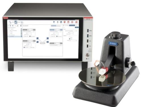
At the pre-component stage, testing must be conducted on the wide bandgap material itself, followed by testing at the wafer stage, to determine the specifications of its behavior. Wide-bandgap semiconductor material research and testing often involve determining the Resistivity and Hall mobility of a sample. The main techniques for measuring these parameters are:
- Van der Pauw method
- Hall Effect measurement
All of these measurements can be made using a parameter analyzer. The Keithley 4200A-SCS Parameter Analyzer includes modules allowing researchers to perform both Van der Pauw resistivity and Hall Effect measurements automatically, saving valuable research time and eliminating the need to purchase a separate system to perform these tests.

- Component-level Testing
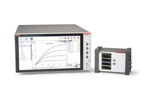
The next stage of testing occurs for components/devices fabricated on the wafer or as a stand-alone component. Device I-V characterization is performed to compare simulation data to actual measurement data. Post-manufacture component testing plays an integral role in the device designer’s creation of data sheets and quality control. It is also used extensively by end customers to validate components against their specifications.
I-V characterization measurements can be made with the 4200A-SCS or with Keithley’s series of high-power source measure units (SMU). Additionally, the 4200A-SCS supports CV measurements. When the 4200A-CVIV Multi-Switch is added to the 4200A-SCS, you gain the following advantages:
- No need to reconnect any cables: reduces user error and permits automated testing.
- Allows measuring circuit level capacitance directly.
- Using bias tee at every terminal eliminates the need for external capacitors or shorts.
- Full CV compensation out to the device under test (DUT).
- Circuit-level Testing
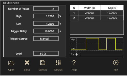
As mentioned above, the switching characteristics of a MOSFET must be tested and characterized after installation in a circuit, typically by means of double-pulse testing using an Arbitrary Function Generator (AFG) to create the pulse test waveform as shown in the diagram. This testing measures parameters that include turn-on and turn-off characteristics as well as thermal behavior. Component manufacturers typically create demonstration boards for internal development use on which they install their MOSFETs for circuit-level testing including the double-pulse test.
To learn more about double pulse testing, we encourage you to watch the video Double Pulse Test with the AFG31000. This video shows how to set up and run a double pulse test using the built-in software on the Tektronix AFG31000 Arbitrary Function Generator. Now you do not need to spend time creating waveforms on a PC or microcontroller. Instead, you can set up your double pulse test in under a minute right on the AFG31000.
-
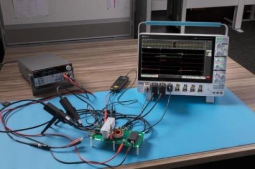
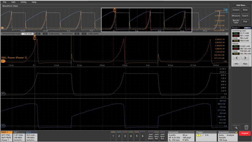
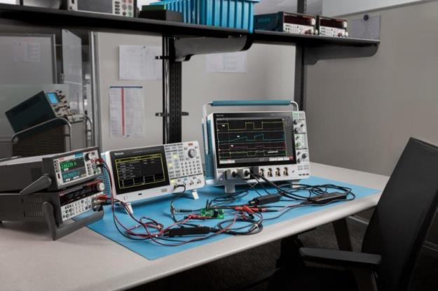
System-level Testing
A fully assembled power module undergoes testing in particular for its operating efficiency using a variety of instruments including oscilloscopes, power supplies, isolated probes and power analysis software as shown in the images below. These instruments and the measurements they provide play a critical role in meeting regulatory guidelines as well as qualifying for certifications such as Energy Star compliance.