THIS APPLICATION NOTE
- Is intended to help designers learn troubleshooting techniques for ESD compliance failures
- Covers some basic theory on ESD
- Describes a basic testing system for ESD troubleshooting, including an H-field probe, oscilloscope and ESD simulator
- Explains how to make measurements and trace ESD current paths in a device under test
This application note uses a 6 Series MSO oscilloscope and near-field probe to illustrate techniques for ESD troubleshooting. Setups and measurements will be practically identical for comparably equipped 4 and 5 Series MSOs, since they share the same controls as the 6 Series MSO. In fact, many of techniques described herein may be used with any professional-grade oscilloscope with appropriate performance.
Introduction
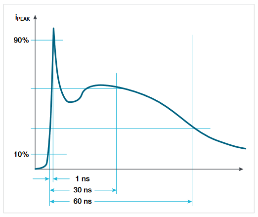
Besides radiated emissions, electrostatic discharge (ESD) is the next most challenging product failure to debug when it comes to EMC compliance. The intermittent nature of the discharges are cause for much of the difficulty in understanding and fixing these failures. Fortunately, there exist ESD simulators that can inject a controlled discharge into a product to force failures. The primary international standards referenced for most products include IEC 61000-4-2 and the U.S. ANSI C63.16, which specify how to set up and perform these ESD tests [References 1 and 2]. ESD generated from a person touching an enclosure or a cable can disrupt the circuits in electronic systems. A typical human-body ESD event creates a high-current discharge into any metallic object as a person’s finger approaches it. The resulting current pulse may amount to several amperes at a very high leading edge with a rise time of less than 1 ns (Figure 1).
The idealized ESD waveform is shown in Figure 1. The rising edge is normally less than 1 ns with a secondary exponentially decaying secondary pulse.

ESD is usually tested between 4 kV and 15 kV for most commercial and consumer products and the discharge waveform follows the "human body model". Depending on the simulator voltage setting, the resulting ESD current can approach over 30 amps of instantaneous current at its peak. Even when troubleshooting in a controlled test environment, it’s difficult to know precisely what part of the circuitry or system is being affected, nor is it clear what path the ESD current actually takes. This is especially an issue with medium to large systems.
As can be observed in Figure 2, the path of ESD current can take several directions, based upon the paths of lowest impedance. Eventually, the current will return back to Earth and to the human or object that created the discharge in the first place.

Unfortunately, it is not possible to see these current pathways, nor deduce what electrical components or active devices may be affected and causing the product compliance failure. However, one method that has worked well in tracing out the discharge path is to inject low-voltage pulses from an ESD simulator into failure points on a product or system. Then, by using a high bandwidth oscilloscope, such as the Tektronix 4, 5 or 6 Series MSO, and small H-field probe, it’s possible to trace the dominant path of current, plus all its branches.

Determine the Path of ESD
In one method, an assistant holds the simulator and triggers it repeatedly into one of the failure points, while another traces the dominant injected currents. If your simulator has a setting for one pulse per second, that would work as well and requires only one person. Generally, the EUT (Equipment Under Test ) will need to be opened up to reveal the internal circuitry and system cabling during this test. Figure 3 shows a block diagram of the test setup.
These paths will commonly include system cables, PC boards, keyboards and displays. The controlled discharges can be traced with the H-field probe by coupling the probe to cables or sweeping the probe around circuit boards. If the current pulse crosses through an IC, or other active device, that should provide a good clue as to the portion of circuitry that is involved with the failure mode of the product or system under test.
For example, let’s assume discharging to a particular I/O connector shell on the EUT causes circuit upset during the ESD test. We’ll want to connect the discharge tip to this connector ground shell to trace the path the ESD current is taking.

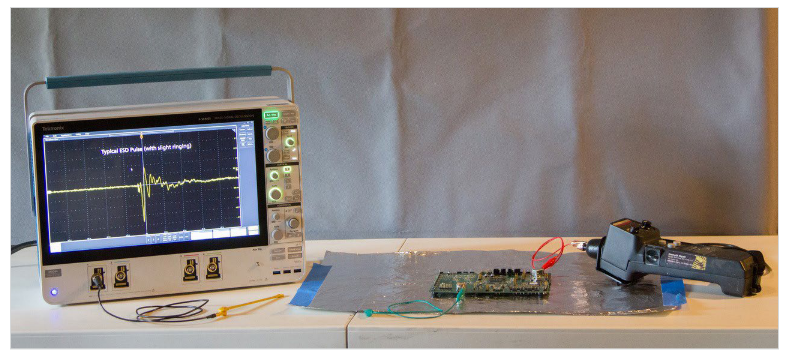
To illustrate this technique, we’ll use a demonstration circuit board (Figures 4 and 5) and connect the simulator contact discharge tip to the I/O connector shell in question using a short clip lead. A drain wire needs to be connected back to the ground plane on the test table to provide a discharge path for the ESD current. Note that for a line operated EUT plugged into the AC line, this drain wire is not necessary, as the ESD currents will return to Earth through the safety ground.

Start by setting up the 4, 5 or 6 Series MSO for 200 mV per division and time base at about 8 ns per division and use Auto acquisition. Plug the H-field probe into channel 1 and set the input impedance to 50 ohms. You may need to adjust the Trigger control slightly positive to catch each pulse. These initial setting are not critical and can be refined during the testing.
Adjusting the ESD simulator for an automatic one pulse per second discharge rate, the H-field probe is scanned around the board to determine the path or paths by observing the relative pulse amplitude. The board does not necessarily need to be powered for this test, but if line-powered, should be plugged in to power to allow ESD currents to return to Earth.
Now, probe around the board and system cables to discover the dominant path or paths of injected current flow. The resulting measurement will show ringing, but the important thing will be to observe the relative amplitude of the pulse as this will indicate the dominant current path.
Figure 6 shows a typical ringing pulse from the H-field probe. The ringing is largely due to the inductance of the long clip leads attached to the EUT resonating with the board-to-plane capacitance and is of no consequence, since the important factor is the general amplitude of the pulse.

Once the path or paths of dominant ESD current are identified, then mitigations may begin. This usually involves blocking or diverting the ESD current. We definitely want to avoid allowing ESD current through our circuit boards. Most line-operated products are connected to Earth through the safety wiring, so often, it’s best to try diverting the ESD current to chassis or the green wire safety ground through better bonding and grounding techniques to chassis. This diversion path should occur “upstream” from any electronic circuitry, usually right at the I/O and power connectors or egress points where ESD is tested. For portable devices, the ESD current should be diverted to the digital return plane at the board I/O and power connectors.
Another technique is to introduce blocking impedances, such as ferrite chokes on any cables that are carrying dominant ESD currents. Usually, a combination of blocking and diverting techniques are sufficient to mitigate ESD compliance failures. Of course, it’s even better to design these mitigations into the product or system at the start!
Summary
Compliance to ESD immunity can be a challenge, especially when discovered near the time of product introduction and market release. Using a high bandwidth oscilloscope, such as the 4/5/6 Series MSO, along with simple probing tools and an ESD simulator can quickly determine the path of ESD currents and help focus mitigation efforts in order to solve last-minute failures.


