Introduction
As a result of the innovations taking place in CPUs, GPUs, accelerators, and switches, the interface in hyperscale datacenters now requires faster data transfers both between compute and memory and onto the network. PCI Express (PCIe®) provides the backbone for these interconnects and is used to build protocols such as Computer Express Link (CXL™) and Universal Chiplet Interconnect Express (UCIe™). The resource-sharing capability of CXL is popularizing memory pulling/expansion across multiple machines and becoming the solution for cache coherent interconnect for processors, providing lowest latency with highest bandwidth. CXL and NVM Express® use the PCIe physical layer (PHY) and leverage the PCIe upper layers, software stack and platform connectivity because of their simplicity and adaptability. UCIe, the latest die-to-die standard, will also build upon PCIe at the protocol layer to provide reliable data transfer, link management and CXL cache coherency. Hence PCIe has become the de-facto standard of interconnect for high-speed data transfers between processing/computing nodes due to its high-speed, low-latency, and low-power attributes.
This paper discusses industry demands for PCI Express 6.0 and future standards, the importance of compliance,how to successfully achieve interoperability through PHY verification, and measurement methodologies for PCIe 6.0 transceivers. Synopsys PCI Express 6.0 IP and Tektronix test and measurement solutions are actively addressing this latest technology inflection point.
Authored By:
David Bouse, PCI Express Technology Lead, Tektronix®
Madhumita Sanyal, Senior Technical Product Manager, Synopsys®
Data Rates Doubling, Again
The PCI-SIG® consortium responsible for the PCIe interface, an open industry standard comprised of over 900 member companies, releases on average a new PCIe generation every three years. Over the past decade, that has led to a regular doubling of the data rate while still maintaining full backward compatibility (Figure 1). The demand for PCIe 6.0.1 was inevitable and inextricably linked to technology demand throughout the compute platform including SSDs to CPU / GPU to accelerators, etc. The standard now introduces multi-level Pulse Amplitude Modulation (PAM4) signaling to achieve a transfer rate of 64 GT/s in one direction on a single lane, and 256 GB/s bi-directionally on a x16 link.
At the 2022 PCI-SIG DevCon, PCI-SIG announced the next-generation PCIe 7.0 specification which doubles the data-rate to 128 GT/s as well as improved power efficiency together with that higher bandwidth. The PCIe 7.0 interface will use 1b/1b flit mode encoding and PAM4 signaling to provide 512 GB/s bi-directional throughput over 16 lanes, thus providing even greater bandwidth while maintaining an extremely low latency interconnect.
Apart from hyperscale data centers, markets like handheld, client, servers, workstations, automotive, embedded systems, industrial applications, etc. that deploy PCIe technology also have very stringent requirements in terms of reliability and cost. As a ubiquitous I/O, PCIe products need to meet such requirements across the entire compute continuum. Verifying that a product is compliant to the PCIe 6.0.1 specification and interoperable with other PCIe devices remains foundational.
| Specifications | Lanes | ||||
| x1 | x2 | x4 | x8 | x16 | |
| 2.5 GT/s (PCIe 1.x +) | 500 MB/S | 1 GB/S | 2 GB/S | 4 GB/S | 8 GB/S |
| 5.0 GT/s (PCIe 2.x +) | 1 GB/S | 2 GB/S | 4 GB/S | 8 GB/S | 16 GB/S |
| 8.0 GT/s (PCIe 3.x +) | 2 GB/S | 4 GB/S | 8 GB/S | 16 GB/S | 32 GB/S |
| 16.0 GT/s (PCIe 4.x +) | 4 GB/S | 8 GB/S | 16 GB/S | 32 GB/S | 64 GB/S |
| 32.0 GT/s (PCIe 5.x +) | 8 GB/S | 16 GB/S | 32 GB/S | 64 GB/S | 128 GB/S |
| 64.0 GT/s (PCIe 6.x +) | 16 GB/S | 32 GB/S | 64 GB/S | 128 GB/S | 256 GB/S |
| 128.0 GT/s (PCIe 7.x +) | 32 GB/S | 64 GB/S | 128 GB/S | 256 GB/S | 512 GB/S |
Figure 1: PCI-SIG Generation Bandwidth
Compliance and Interoperability Testing
PCI-SIG compliance and interoperability testing is crucial for PCIe 6.0.1 Integrators. Design verification, PHY validation,and PCI-SIG compliance testing and interoperability with the PCIe ecosystem collectively pave the way for lowering integration risk and improving overall product quality.
There are various PCIe system topologies tailored for servers, storage boxes, GPU trays, and many different types of physical channels with different connector type and count. All configurations need to meet the PCIe 6.0.1 channel insertion loss budget of 32 dB at 16 GHz Nyquist. The PCIe 6.0.1 insertion loss budget of 32 dB is shared with ~23.5 dB for a Root Complex (system) and 8.5 dB for a Non-Root Complex (e.g., CEM add-in card (AIC). The example of a CEM AIC includes both AIC PCB traces and a Non-Root Complex package loss of 4.6 dB. System designers are left with ~15.7 dB budget to design their board traces via capacitors from RP pads on the PCB to the AIC connectors. Due to the minimum allowable distance without additional componentry between the PCIe root device (e.g., CPU) and the end device (e.g., GPU), motherboards will likely include retimers and thicker PCBs comprised of higherquality materials than we saw with prior generations of the interface. Bandwidth doubling from 32 GT/s to 64 GT/s and beyond (128 GT/s for Gen7) and the backward-compatibility requirement in PCIe for legacy channels (PCB + connectors + add-in card, etc.) add to this complexity.
Temperature and humidity effects can cause ±10% insertion loss variation with advanced PCB material and ±25% variation with mainstream PCB material. Ecosystem development must be aware of this and the PHY must compensate for impedance discontinuities and PVT variations in insertion loss. Channel equalization techniques can be done adaptively and continuously in the background to compensate and track voltage, temperature, and humidity drift over time and the PHY must optimize for long and short channels and compensate worst case scenarios which adds operating margin. Hence extensive test validation and interoperability with the ecosystem is essential to validate PHY robustness.
New Measurement Methods for PAM4 Signaling
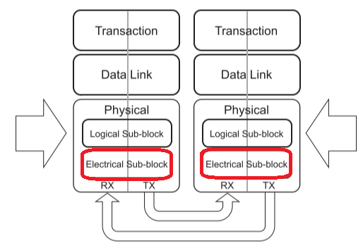
The PCI Express 6.0.1 Base Specification segments the PHY Layer into a logical sub-block and electrical sub-block (Figure 2). Validation of the electrical sub-block is a prerequisite to full validation of the PHY Layer and will be the focus of this paper. The electrical sub-block is comprised of a transmitter (Tx), receiver (Rx), reference clock (Refclk), and channel requirements. Transceivers (Tx & Rx) supporting the new 64 GT/s data rata rate must also maintain backwards compatibility with the lower speeds of (2.5, 5.0, 8.0, 16.0, & 32.0) GT/s. The pulse amplitude modulation method introduced in 6.0.1 requires four distinct signal levels (PAM4) which allows transmission of two bits of information within a single unit interval (UI). The move from NRZ (two signal levels) to PAM4 ensures the channel loss is consistent with PCIe 5.0 (32 GT/s) as the Baud Rate is 32 Gb/s for both speeds with a shared Nyquist frequency of 16 GHz.
The change in signaling scheme from NRZ to PAM4 reduces the vertical eye diagram opening by 33% as we move from 2 signal levels to 4 signal levels. There are now 3 eye diagrams to consider instead of a single eye under NRZ. This reduction in noise margin exacerbates cross-talk interferences, signal reflections, and power supply noise. To mitigate the increased noise sensitivity, PCIe 6.0.1 also adopted Gray coding to minimize bit errors and pre-coding to reduce burst error propagation. DAC and ADC/DSP-based Tx and Rx equalization techniques can be used to correct for the compensable impairments such as inter-symbol interference (ISI) where adjacent bits blur together due to channel impacts, including loss and reflection. The PCIe 6.0.1 specification has introduced the Signal-to-Noise Distortion Ratio (SNDR) to help quantify this new design challenge.
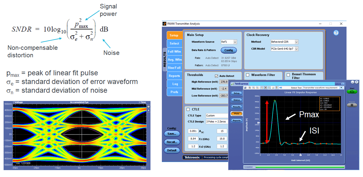
SNDR builds upon the long-established SNR measurement but introduces a component called “sigma e” to capture the non-compensable impairments within the electrical signal. To simplify design and intuitive understanding, we rely heavily on linear models which only approximate the physical world. Non-linear behavior does exist within PCIe transceivers and communication channels. The standard moves to capture this impact with the SNDR “sigma e” term. Techniques have been borrowed from IEEE standards and customized for this 64 GT/s PCIe measurement. The pulse response is created from a PRBS data pattern waveform using IEEE’s linear fit pulse response method which becomes central to determining the signal amplitude and “sigma e”. Accurate SNDR measurements require a 50 GHz bandwidth real time oscilloscope to capture the signal and DSP software for the waveform post-processing (Figure 3).
One anticipated non-linearity for PAM4 signaling appears when the transmitted signal levels are unevenly spaced. Assuming a static amplitude, this will impair one or more of the 3 eye diagrams and lead to increased bit errors. Characterization of this phenomenon during post-silicon validation allows transceiver adjustments or design changes to increase the level linearity. To address this, the PCIe standard introduced Ratio of Level Mismatch (RLM) for the first time to better understand and improve PAM4 transmitter performance. This Base specification measurement is expected to extend into system level validation for different form factors including Card Electro Mechanical (CEM) commonly implemented for graphics cards and network interface cards (NICs).
Moving from voltage- to timing-related challenges has significant implications for achieving a stable link at the latest PCIe 6.0.1 data rate. The nominal slope of signals moving from adjacent levels (e.g., level 1 to level 2) will be smaller than a transition from level 0 to level 3, resulting in a greater transfer of vertical noise to timing jitter. Additionally, there is an inherent eye width reduction with an increased number of possible level transitions to consider. Advanced measurement instrument (e.g., real time oscilloscope) noise characterization and compensation techniques have been comprehended for the first time in a PCIe standard to mitigate measurement related noise and improve accuracy in voltage and timing measurements such as uncorrelated jitter.
Measurement methodologies established for PCIe 4.0 and 5.0 receivers are expanded with PCIe 6.0.1 Rx calibration and test. A worst “stressed eye” signal is created using the highest channel loss allowed and delivered to an Rx under test to quantify performance. The Rx will digitize the analog signal and then use loopback mode to re-transmit the bit stream from the corresponding Tx for direct bitby-bit comparison to determine a bit error rate (BER) or measure jitter tolerance (JTOL) of different sinusoidal jitter (Sj) frequencies. Receivers operating at 64 GT/s are required in order to track the increasing amount of jitter below 10 MHz and 0.05 UI of higher frequency. Clocking architectures with independent clocks between the upwards and downwards facing ports require increased tolerance for handling spread spectrum clocking (SSC) at 33 kHz.
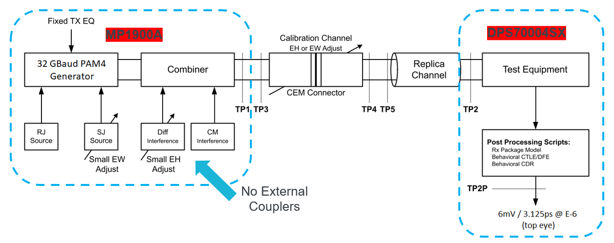
Calibration of the stressed eye signal is a complex aspect of the physical layer validation and involves a bit error rate tester (BERT), physical channel, real time oscilloscope (scope), and numerous DSP software packages. Ultimately, this is a calibration of the BERT’s Pulse Pattern Generator (PPG) which is acting as a PCIe Tx. Figure 4 depicts this calibration procedure. The goal is to establish an eye diagram which is embedded to the latch of a behavioral Rx defined in the base specification including a CDR and behavioral Rx equalizer. The allowable range for top eye height and eye width is found where channel loss, noise, and jitter are knobs to achieve the target eye. ISI from the channel adjustments provide the largest adjustments to the eye while Sj and cross talk using differential mode interference serve as fine-tuning mechanisms. The industry increasingly relies on software automation to comprehend and achieve the stressed eye calibration for receiver testing.
PCIe 6.0 Solutions
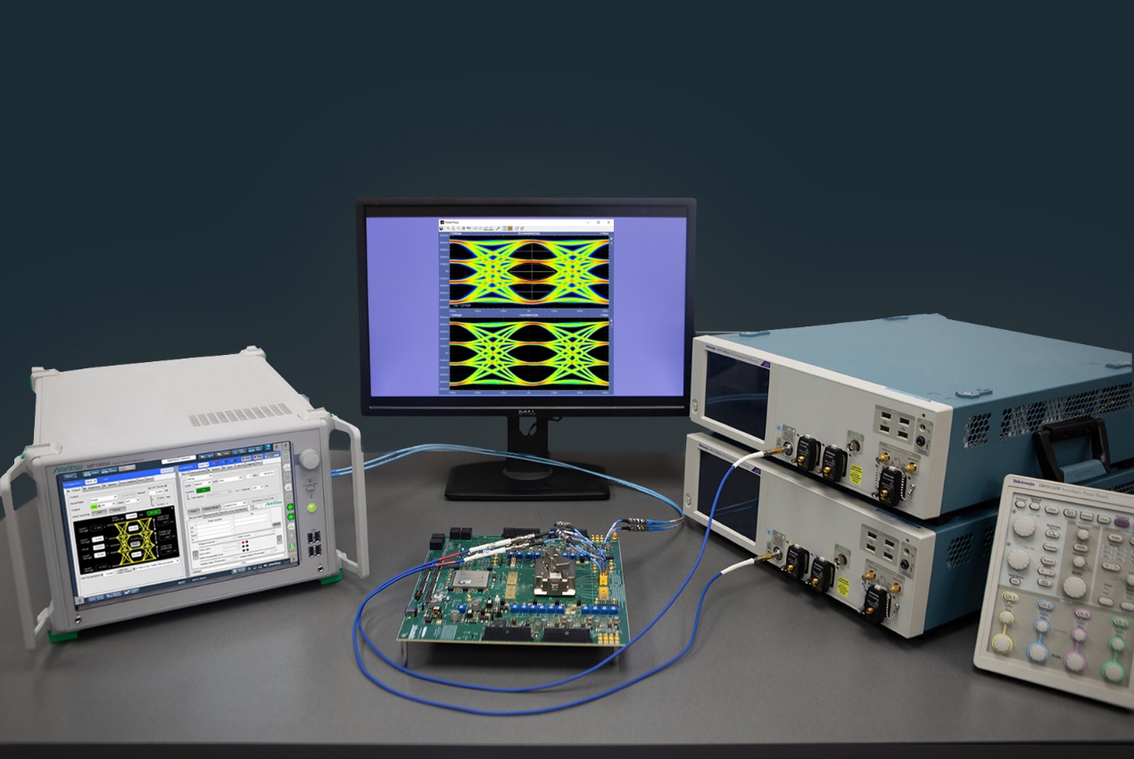
Interoperability continues to be a pillar of the success of PCIe technology and has led to the extensive proliferation and adoption of newly emerging technologies such as CXL as well as inclusion in future chiplet (die-to-die) designs like UCIe. Achieving interoperability starts with IP design or selection and involves testing at a Base specification and system level to ensure that devices, often from different vendors, can properly train the link and maintain stability across operating voltages and temperatures. The achievable yield must also be considered for high volume manufacturing-based products. As an example, for validation of the Synopsys PCI Express 6.0 IP, the test setup applied here is comprised of a Tektronix DPS77004SX oscilloscope together with Tektronix test automation software and an Anritsu MP1900A BERT (Figure 5).
Synopsys offers complete PCI Express Controller, PHY and Verification IP solutions across all generations of the standard with proven silicon in customer products targeting a wide range of applications including Re-timer, Flash Controller, Accelerator, SSD U.2/U.3, PCIe switch, and Smart NIC.
Synopsys IP has achieved numerous successful third-party interoperability. Tektronix offers a complete PCI Express 6.0 Base Tx/Rx automated solution with backwards compatibility for lower data rates and form factor specific testing.