Introduction
Many critical applications demand the ability to measure very low currents such as picoamps or less. These applications include determining the gate leakage current of FETs, testing sensitive nano-electronic devices, and measuring leakage current of insulators and capacitors.
The Model 4200-SCS Semiconductor Characterization System, when configured with the optional Model 4200-PA Remote Preamp, offers exceptional low current measurement capability with a resolution of 1E-16A. Making low current measurements successfully depends not only on using a very sensitive ammeter like the Model 4200-SCS's, but on choosing the proper settings in the system's Keithley Interactive Test Environment (KITE) software, using low noise fixtures and cabling, allowing sufficient settling time, and using techniques that prevent unwanted currents from reducing measurement accuracy. This application note describes Keithley's best-known methods recommendations for optimizing low current measurements using the Model 4200-SCS
Measuring the Offset Current of the System
One of the first steps in setting up a system for making ultra low current measurements is to determine the offset and leakage current of the entire measurement system, which includes the 4200-SCS itself, the connecting cables, switch matrix, test fixtures, and probes. This identifies the noise floor limit of the entire system and sets a starting point for making improvements to the system, if possible. Start by measuring the offset of the Source-Measure Units (SMUs) and then continue to add components of the measurement circuit until everything is connected except the device under test (DUT).The measurements are made directly by the 4200-SMU with the 4200-PA Remote PreAmp using the KITE software.
Internal Offsets
The ideal ammeter should read zero current when its input terminals are left open. Practical ammeters, however, do have some small current that flows when the input is open. This current, which is known as the input offset current, is generated by bias currents of active devices and by leakage currents through insulators within the instrument. The offset current generated within the SMU is included in the Model 4200-SCS's specifications. As shown in Figure 1, the input offset current adds to the measured current so the meter measures the sum of the two currents:
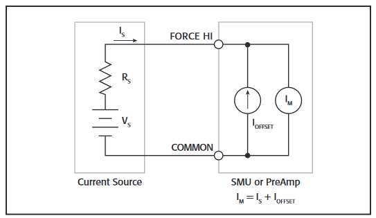
The offset of each 4200-SMU with the 4200-PA preamp is measured with nothing connected to the Force HI and Sense HI terminals except metal caps. These three-lug metal caps are included with the system. Before taking any measurements, the SMUs should be warmed up with the metal caps connected to the Force HI and Sense HI terminals of the preamps for at least one hour. If the system has KTEI software version 7.1 or later installed, the offset current can be measured using the project called "LowCurrent" located on the system in this directory:C:\S4200\kiuser\Projects\LowCurrent
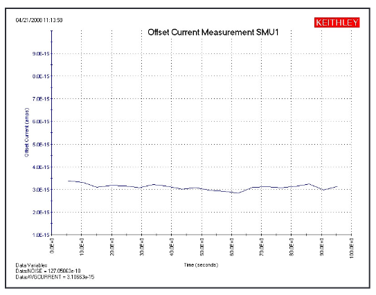
Open this project and select the SMU1offset ITM. Click on the graph tab and run the test. The results should be similar to the graph shown in Figure 2. It may be necessary to use the Auto Scale function to scale the curve appropriately. The Auto Scale function can be found by right-clicking on the graph. With the 4200-PA preamp connected to the SMU, the offset current should be in the femtoamp range. The current offset can be positive or negative. Verify these results with the published ammeter specifications for the Model 4200-SCS.
This test should be repeated using a separate ITM for each SMU in the system. The LowCurrent project has ITMs for performing offset current measurements on four SMUs with preamps.
It is also easy to measure the offset current for systems running versions of the KTEI software earlier than 7.1. Follow these steps to create a test to perform this measurement on SMU1:
- Within a project that has already been created, open a new Device Plan for a generic 2-terminal device.
- Create a new ITM called SMU1Offset. Select SMU1 for terminal A and the GNDU for terminal B.
-
Set up the following in the Definition Tab:
SMU Force/Measure Configuration: Voltage bias 0V,10pA fixed current range.
Timing Menu: Quiet Speed, Sampling Mode, 0s Interval,20 Samples, 1s Hold Time, Timestamp Enabled checked
Formulator: Create a formula to measure noise using the standard deviation function, NOISE=STDDEV(A1).
Also create a formula to measure the average offset current: AVGCURRENT=AVG(A1).
-
Set up the following in the Graph Tab (right-click on graph):
Define Graph: X-axis: Time
Y1-axis: Current (A1)
Data Variables: Select NOISE to appear on graph. Select AVGCURRENT to appear on graph.
Once the test is configured, save the test and run it. The results should be similar to those shown in Figure 2. Repeat the test for all the SMUs in the system
The input offset current specification can be optimized by performing an auto calibration procedure in KITE. To perform an SMU auto calibration, go to the KITE Tools menu and click on SMU Auto Calibration. Before performing the auto calibration,allow the system to warm up for at least 60 minutes after power-up. Nothing should be connected to the SMU Force HI and Sense HI terminals except a metal cap. The auto calibration routine adjusts the current and voltage offsets for all source and measurement functions of all SMUs in the system. This should not be confused with a full system calibration, which should be performed once per year at the Keithley factory.
The offset current measurement can be repeated once the SMU auto calibration has been performed.
External Offsets
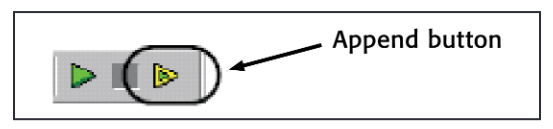
Once the offset current of the ammeter has been determined,verify the offset of the rest of the system by repeating (using the Append Run button shown in Figure 3) the current (at zero volts) vs. time graph after adding each piece of the test circuit.Finally, make a measurement to the end of the probe in the "up" position or to the test fixture with no device connected.This process will help determine any trouble spots, such as a shorted cable or instability in the measurement circuit.However, be aware that connecting and disconnecting cables generates current in the circuit. For making ultra-low current measurements, it may be necessary to wait from a few minutes to hours for the spurious currents to decay after changing connections in the test circuit. Figure 4 illustrates a graph showing the offset of 1) just the SMU with a capped Force HI terminal, 2) with only a triax cable on the preamp, and finally 3) through the Keithley 7174A Low Current Switch Matrix to a probe station with a probe in the "up" position.

This test should be repeated to determine any leakage circuit in the measurement circuit by applying a test voltage when generating the current vs. time graph. Rather than applying a zero volt bias, use the test voltage that will be used in the actual measurements of the DUT. Any leakage current in the test fixtures and cables will now be measured and graphed. If the leakage appears to be too high, adjustments can be made to the measurement circuit to reduce the leakage current. Refer to the section titled "Leakage Current and Guarding," which describes ways to reduce leakage current.
Sources of Measurement Errors and Ways to Reduce Them
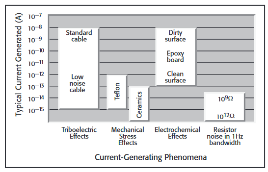
Once the current offsets, leakage current, and any instability have been determined, taking steps to reduce measurement errors will help improve measurement accuracy. These sources of error include insufficient settling time, electrostatic inference,leakage current, triboelectric effects, piezoelectric effects,contamination, humidity, ground loops, light, and source impedance. Figure 5 summarizes the magnitudes of some of the generated currents discussed in this section.
Settling Time and Timing Menu Settings
The settling time of the measurement circuit is particularly important when making low current and high resistance measurements. The settling time is the time that a measurement takes to stabilize after the current or voltage is applied or changed. Factors affecting the settling time of the measurement circuit include the shunt capacitance (CSHUNT) and the source resistance (RS). The shunt capacitance is due to the connecting cables, test fixtures, switches, and probes. The higher the source resistance of the DUT, the longer the settling time. The shunt capacitance and source resistance are illustrated in the measurement circuit in Figure 6
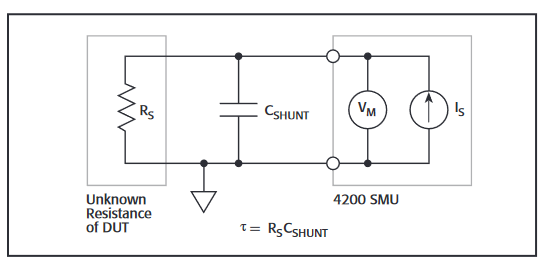
The settling time is the result of the RC time constant, or τ,where:
τ = RSCSHUNT
An example for determining the settling time can be calculated as follows, if CSHUNT = 10pF and RS = 1TΩ, then:
τ = 10pF × 1TΩ = 10 seconds
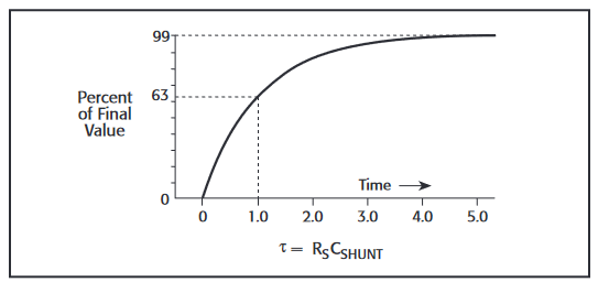
Therefore, a settling time of five τ, or 50 seconds, would be required for the reading to settle to within 1% of final value! Figure 7 shows the exponential response of a step voltage into an RC circuit. After one time constant (τ = RC), the voltage rises to within 63% of final value.
To make successful low current measurements, it's important to add sufficient time for each measurement, particularly when sweeping voltage. This settling time can be added in the Timing menu in the Sweep Delay field for the Sweeping Mode or the Interval time field for the Sampling Mode. To verify how much interval time to add, measure the settling time of the DUT by plotting the current vs. time to a stepped voltage. The stepped voltage should be the bias voltage that will be used in the actual measurement of the DUT. The ITMs in the LowCurrent project can be used to perform the settling time measurement. The #Samples in the Timing Menu will probably need to be increased to ensure settled readings will be displayed on the graph. When making low current measurements, use the Quiet Speed Mode or add extra filtering in the Timing Menu. Keep in mind that there is a noise/speed trade-off. With more filtering and delays, there will be less noise but a slower measurement speed.
Electrostatic Interference and Shielding
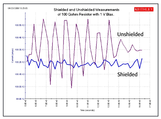
Electrostatic coupling or interference occurs when an electrically charged object approaches the circuit under test. At low impedance levels, the effects of the interference aren't noticeable because the charge dissipates rapidly. However, high resistance materials don't allow the charge to decay quickly, which may result in unstable, noisy measurements. Typically, electrostatic interference is an issue when making current measurements ≤1nA or resistance measurements ≥1GΩ.
To reduce the effects of the fields, the circuit being measured can be enclosed in an electrostatic shield. Figure 8 illustrates the dramatic difference between an unshielded and a shielded measurement of a 100GΩ resistor. The unshielded measurements are much noisier than the shielded measurements.
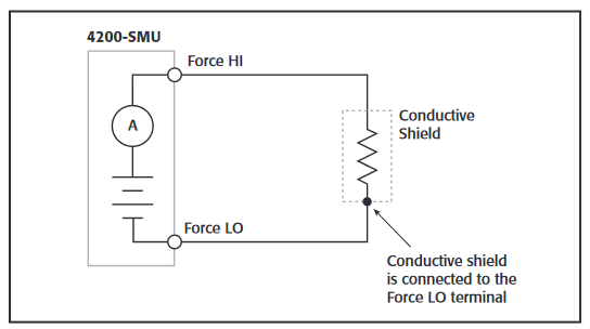
The shield can be just a simple metal box or meshed screen that encloses the test circuit. Commercial probe stations often enclose the sensitive circuitry within an electrostatic shield. The shield is connected to the measurement circuit LO terminal,which is not necessarily earth ground. In the case of the Model 4200-SCS, the shield is connected to the Force LO terminal as shown in Figure 9.
To minimize error currents due to electrostatic coupling:
- Shield the DUT and connect the enclosure electrically to the test circuit common, the Force LO terminal of the 4200-SCS.
- Keep all charged objects (including people) and conductors away from sensitive areas of test circuit.
- Avoid movement and vibration near the test area
Leakage Current and Guarding
Leakage current is an error current that flows (leaks) through insulation resistance when a voltage is applied. This error current becomes a problem when the impedance of the DUT is comparable to that of the insulators in the test circuit. To reduce leakage currents, use good quality insulators in the test circuit,reduce humidity in the test lab, and use guarding.
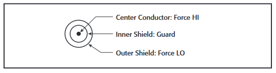
The guard is a conductor driven by a low impedance source whose output is at or near the same potential as the high impedance terminal. The guard terminal is used to guard test fixture and cable insulation resistance and capacitance. The guard is the inside shield of the triax connector/cable illustrated in Figure 10
Guarding should not be confused with shielding. Shielding usually implies the use of a metallic enclosure to prevent electrostatic interference from affecting a high impedance circuit.Guarding implies the use of an added low impedance conductor,maintained at the same potential as the high impedance circuit,which will intercept any interfering voltage or current. A guard doesn't necessarily provide shielding. The following paragraphs outline two examples of guarding: 1) using guarding to reduce the leakage due to a test fixture and 2) using guarding to reduce leakage currents due to cabling.
Figure 11 shows how the guard can eliminate the leakage current that may flow through the stand-off insulators in a test fixture. In Figure 11a, the leakage current (IL flows through the stand off insulators (RL). This leakage current is added to the current from the DUT (IDUT) and is measured by the SMU ammeter (IM), adversely affecting the accuracy of the low current measurement.
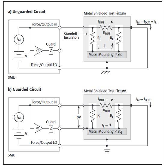
In Figure 11b, the metal mounting plate is connected to the guard terminal of the SMU. The voltages at the top and bottom of the stand off insulator are nearly at the same potential (0V drop), so no leakage current will flow through the standoffs to affect the measurement accuracy. For safety purposes, the metal shield must be connected to earth ground because the metal mounting plate will be at the guard potential.
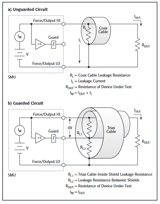
Guarding can also be used to reduce leakage currents in cabling. Figure 12 illustrates how a driven guard prevents the leakage resistance of a cable from degrading low current measurements. In the unguarded configuration, the leakage resistance of the coax cable is in parallel with the DUT (RDUT),creating an unwanted leakage current (IL). This leakage current will degrade very low current measurements.
In the guarded circuit, the inside shield of the triax cable is connected to the guard terminal of the SMU. Now this shield is driven by a unity-gain, low impedance amplifier (guard).The difference in potential between the Force HI terminal and the Guard terminal is nearly 0V, so the leakage current (IL) is eliminated.
To see the results of using triax cable vs. coax cable when making a very high resistance measurement, Figure 13 shows the results of measuring current vs. time of a 10V step function into a 100GΩ resistor. The triax cable enables guard, improving the measurement in two ways: 1) it reduces the effective cable capacitance and thus decreases the RC time constant or settling time of the measurement, and 2) it prevents the leakage resistance of the cable from degrading the measurement accuracy.
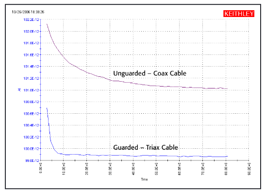
As you can see from the graph in Figure 13, using triax cables with guarding resulted in measured currents that had lower leakage (a few picoamps lower) and had a faster settling time (about ten times faster).
If the SMUs must be connected to a test fixture with BNC connectors, use Keithley triax cables from the SMUs to the test fixture, and then BNC to triax adaptors (with guard removed) to attach the cables to the test fixture.
SMU Connections to DUT
In addition to using shielding and guarding when making connections to the DUT, it is very important to connect the appropriate terminal of the 4200-SCS to the appropriate terminal of the device. Improper connections of the SMU Force HI and Force LO terminals can cause current offsets and unstable measurements. These errors are due to common mode current.
In general, always connect the high impedance terminal (Force HI) of the SMU to the highest resistance point of the circuit under test. Likewise, always connect the low impedance terminal (Force LO) of the 4200-SCS to the lowest resistance point of the circuit under test. The lowest resistance point may be a common terminal or earth ground. If the Force HI terminal is connected to the lowest resistance point, common mode current can flow through the measurement circuit.
Figure 14 illustrates both a proper and an improper measurement connection. Figure 14a indicates a proper connection because the Force HI terminal of the 4200-SMU is connected to the gate of the device on a wafer, and the Force LO terminal is connected to the grounded chuck. The gate terminal on the wafer is the highest impedance point and the grounded chuck is the low impedance point, so this circuit is a proper connection. Note that the common mode current flows from the Force LO terminal of the SMU to the grounded chuck; however,the current does not flow through the ammeter, and therefore does not affect the measurement.
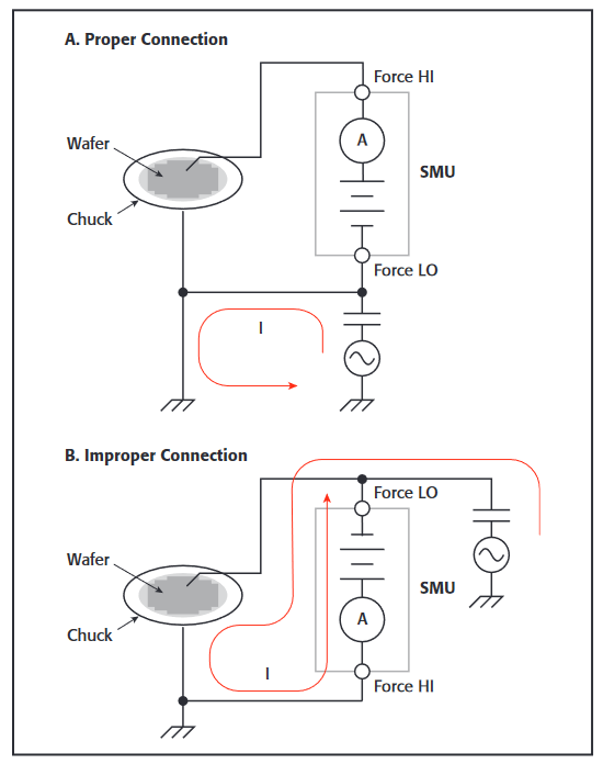
Figure 14b illustrates an improper connection with the Force LO terminal of the SMU connected to the high impedance gate terminal and the Force HI terminal of the SMU connected to the grounded chuck. In this case, the common mode current will flow through the SMU as well as the DUT. This will result in inaccurate, even unstable measurements.
Triboelectric Effects
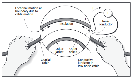
Triboelectric currents are generated by charges created between a conductor and an insulator due to friction. Here, free electrons rub off the conductor and create a charge imbalance that causes the current flow. This noise current can be in the range of tens of nanoamps. Figure 15 illustrates the flow of triboelectric current.
The triax cables supplied with the 4200-SCS greatly reduce this effect by using graphite-impregnated insulation beneath the outer shield. The graphite provides lubrication and a conducting cylinder to equalize charges and minimize charge generated by frictional effects of cable movement. However, even this type of triax cable creates some noise when subjected to vibration and expansion or contraction. Therefore, all connections should be kept short, away from temperature changes (which would create thermal expansion forces), and preferably supported by taping or wiring the cable to a non-vibrating surface such as a wall, bench,or rigid structure.
Other techniques should also be employed to minimize movement and vibration problems:
- Remove or mechanically decouple vibration sources such as motors, pumps, and other electromechanical devices.
- Securely mount or tie down electronic components, wires,and cables.
- Mount the preamps as close as possible to the DUT.
Piezoelectric and Stored Charge Effects
Piezoelectric currents are generated when mechanical stress is applied to certain crystalline materials when used for insulated terminals and interconnecting hardware. In some plastics,pockets of stored charge cause the material to behave in a manner similar to piezoelectric materials. An example of a terminal with a piezoelectric insulator is shown in Figure 16.
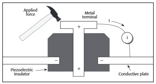
To minimize these effects, remove mechanical stresses from the insulator and use insulating materials with minimal piezoelectric and stored charge.
Contamination and Humidity Effects
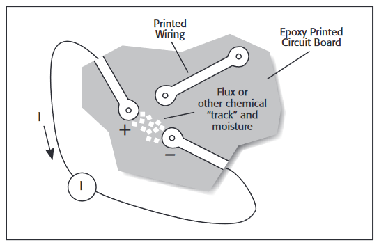
The insulation resistance of test fixtures can be dramatically reduced by high humidity or ionic contamination. High humidity conditions occur with condensation or water absorption, while ionic contamination may be the result of body oils, salts, or solder flux. A reduction in insulation resistance can have a serious effect on high impedance measurements. In addition,humidity or moisture can combine with any contaminants present to create electrochemical effects that can produce offset currents. For example, commonly used epoxy printed circuit boards, when not thoroughly cleaned of etching solution, flux, or other contamination, can generate currents of a few nanoamps between conductors (see Figure 17).
To avoid the effects of contamination and humidity, select insulators that resist water absorption, and keep humidity to moderate levels (ideally <50%). Also, be sure all components and test fixturing in the test system are kept clean and free of contamination.
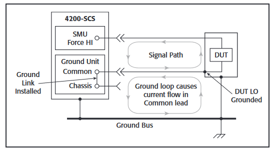
Ground Loops
Ground loops can generate spurious signals that may be a DC offset or an AC signal (usually line frequency or multiples of line frequency). Ground loops are caused by multiple grounds in the test circuit. A typical example of a ground loop can be seen when a number of instruments are plugged into power strips on different instrument racks. Frequently, there is a small difference in potential between the ground points, which can cause large currents to circulate and create unexpected voltage drops.
The configuration shown in Figure 18 shows a ground loop that is created by connecting both the 4200 signal common (Force LO) and DUT LO to earth ground. A large ground current flowing in the loop will encounter small resistances, either in the conductors or at the connecting points. This small resistance results in voltage drops that can affect performance.
To prevent ground loops, the test system should be connected to ground at only a single point. If it is not possible to remove the DUT ground, the ground link between the 4200 GNDU COMMON terminal and chassis ground should be removed, as shown in Figure 19.
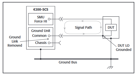
If a ground loop is suspected, unplug the suspect instrument from the AC power and try making a sensitive current measurement to verify the problem is gone. To eliminate ground loops,make as few grounds as possible, preferably, no more than one.
Light
Some components such as diodes and transistors are excellent light detectors. Consequently, these components must be tested in a light-free environment. To ensure measurement accuracy,check the test fixture for light leaks at door hinges, tubing entry points, and connectors or connector panels.
Noise and Source Impedance
Noise can seriously affect sensitive current measurements. Both the source resistance and the source capacitance of the DUT can affect the noise performance of the SMU.
The source resistance of the DUT will affect the noise performance of the SMU's feedback ammeter. As the source resistance is reduced, the noise gain of the ammeter will increase. Figure 20 shows a simplified model of a feedback ammeter.
In this circuit:
RS = source resistance
CS = source capacitance
VS = source voltage
VNOISE = noise voltage of the ammeter
RF = feedback resistor
CF = feedback capacitance
The noise gain of the circuit can be given by this equation:
Output VNOISE = Input VNOISE(1+RF/RS)
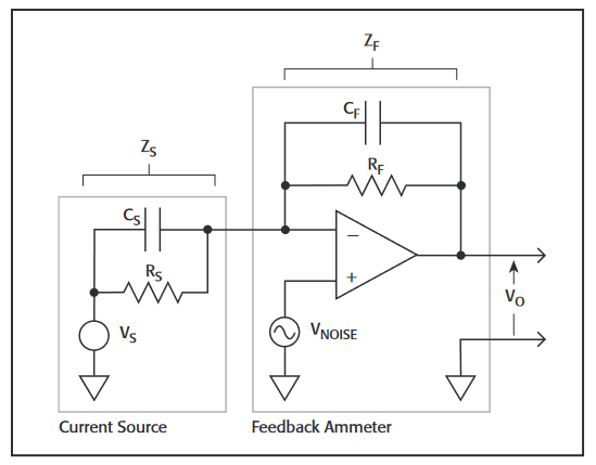
Note that as the source resistance (RS) decreases, the output noise increases. Because decreasing the source resistance can have a detrimental effect on noise performance, there are minimum recommended source resistance values based on the current measurement range, which are summarized in Table 1.
Table 1. Minimum Recommended Source Resistance Values
| Range | Minimum Recommended Source Resistance |
| 1pA to 100pA | 1GΩ to 100GΩ |
| 1nA to 100nA | 1MΩ to 100MΩ |
| 1µA to 100µA | 1kΩ to 100kΩ |
| 1mA to 100mA | 1Ω to 100Ω |
The source capacitance of the DUT will also affect the noise performance of the SMU. In general, as source capacitance increases, so does the noise gain. Although there is a limit as to the maximum source capacitance value, it’s usually possible to measure at higher source capacitance values by connecting a resistor or a forward-biased diode in series with the DUT. The diode acts like a variable resistance, low when the charging current to the source capacitance is high, then increasing in value as the current decreases with time.
Compensating for Offsets
After external errors have been determined and reduced, if possible, the internal and external offsets of the test system can be subtracted from future measurements. First, perform the SMU auto calibration with the capped input as described. Then, determine the offsets for each SMU to the probe tip. This average offset current can be subtracted from subsequent current measurements in other projects using the Formulator tool in the software. For making very low current measurements, the average offset current should be remeasured periodically (at least monthly).
Conclusion
When configured with the optional Model 4200-PA Remote PreAmps, the Model 4200-SCS Semiconductor Characterization System can measure accurately currents of picoamps or less.The offset current of the entire measurement system should be measured to determine the system's limitations, so it can be adjusted if necessary. Sources of measurement errors can be reduced by using techniques such as shielding, guarding, and proper grounding of instruments, and by choosing appropriate settings in the KITE software, including allowing sufficient settling time. Keithley's Low Level Measurements Handbook provides further information on optimal low current measurement techniques.
Find more valuable resources at TEK.COM
Copyright © Tektronix. All rights reserved. Tektronix products are covered by U.S. and foreign patents, issued and pending. Information in this publication supersedes that in all previously published material. Specification and price change privileges reserved. TEKTRONIX and TEK are registered trademarks of Tektronix, Inc. All other trade names referenced are the service marks, trademarks or registered trademarks of their respective companies.
No. 2959 05.28.08