Свяжитесь с нами
Живой чат с представителями Tektronix. С 9:00 до 17:00 CET
Позвоните нам
С 9:00 до 17:00 CET
Загрузить
Загрузить руководства, технические описания, программное обеспечение и т. д.:
Обратная связь
Wide Bandgap Semiconductor Materials Research – A New World of Challenges
The effort to boost device density and performance while reducing power consumption has led to research into unique two-dimensional (2-D) solids with high carrier mobility, higher conductivity, as well as organic semiconductors and nano-scale devices. The desire for greener power generation solutions is spurring investigation into higher temperature superconductors and the power semiconductors essential to power conversion. Materials like gallium arsenide (GaAs) and silicon carbide (SiC) will be crucial to future power transmission technologies. Materials research is also central to boosting the conversion efficiency and power output of solar cells. Tektronix and Keithley have led the world in creating some of the most sensitive semiconductor testing instrumentation, enabling researchers, scientists, and engineers to unlock the potential of new materials.
Techniques for Repeatable Material Science Measurements
Four-point collinear probe resistivity configuration.
Learn More:
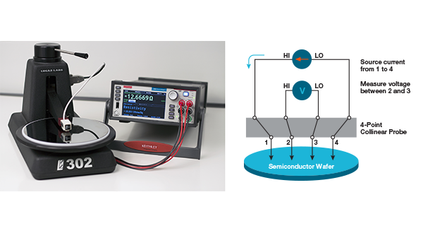
Four-Point Probe Measurement Technique
Semiconductor material research and device testing often involve determining the resistivity and Hall mobility of a sample. The resistivity of a semiconductor material is primarily dependent on the bulk doping. In a device, the resistivity can affect the capacitance, the series resistance, and the threshold voltage. The resistivity of the semiconductor is often determined using a four-point probe technique. Using four probes eliminates measurement errors due to the probe resistance, the spreading resistance under each probe, and the contact resistance between each metal probe and the semiconductor material.
van der Pauw Resistivity Measurement Method
The resistivity of semiconductor materials is often derived using the van der Pauw (vdp) technique. This four-wire method is used on small, flat shaped samples of uniform thickness with four terminals. he van der Pauw method involves applying a current and measuring voltage using four small contacts on the circumference of a flat, arbitrarily shaped sample of uniform thickness. This method is particularly useful for measuring very small samples because geometric spacing of the contacts is unimportant. Effects due to a sample's size, which is the approximate probe spacing, are irrelevant. Using this method, the resistivity can be derived from a total of eight measurements that are made around the periphery of the sample.
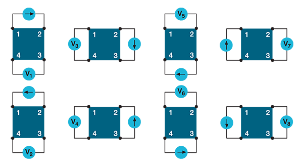
Van der Pauw Resistivity Conventions.
Learn More:
Four-Probe Resistivity and Hall Voltage Measurements with the Model 4200-SCS
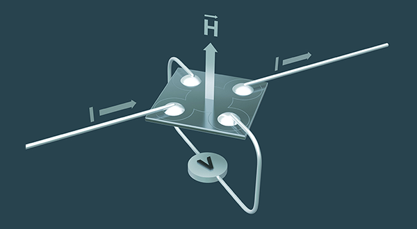
Hall Effect Measurements in Materials Characterization
Hall effect measurements are important to semiconductor material. With an applied magnetic field, the Hall voltage can be measured. A Hall effect measurement system can actually be used to determine quite a few material parameters, but the primary one is the Hall voltage (VH). Other important parameters such as carrier mobility, carrier concentration (n), Hall coefficient (RH), resistivity, magnetoresistance (R ), and the conductivity type (N or P) are all derived from the Hall voltage measurement. Hall effect measurements are useful for characterizing virtually every material used in producing semiconductors, such as silicon (Si) and germanium (Ge), as well as most compound semiconductor materials, including silicon-germanium (SiGe), silicon-carbide (SiC), gallium arsenide (GaAs), aluminum gallium arsenide (AlGaAs), indium arsenide (InAs), indium gallium arsenide (InGaAs), indium phosphide (InP), cadmium telluride (CdTe), and mercury cadmium telluride (HgCdTe).