Introduction
Source-measure units (SMUs), such as the Keithley Model 2651A High Power System SourceMeter instrument, are the most flexible and most precise equipment for sourcing and measuring current and voltage. Because of this, they are widely used to test semiconductor devices such as MOSFETs, IGBTs, diodes, high brightness LEDs, and more.
With today's focus on green technology, the amount of research and development being done to create semiconductor devices for power management has increased significantly. These devices, with their high current/high power operating levels, as well as their low On resistances, require a unique combination of power and precision to be tested properly. A single Keithley Model 2651A is capable of sourcing up to 50A pulsed and 20A DC. For applications requiring even higher currents, Model 2651As can be combined to extend their operating range to 100A pulsed.
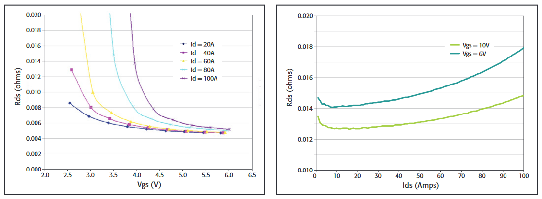
This application note demonstrates how to collect Rds (on) measurement data from a power MOSFET device by using a pulsed current sweep to test up to 100A (see Figure 1); however, it can be easily modified for use in other applications. The document is divided into three sections: theory, implementation, and example.
Theory
Kirchhoff's Current Law says that the sum of the currents entering a node is equal to the sum of the currents leaving the node. In Figure 2, two current sources representing SMUs and a device under test (DUT) are connected in parallel.
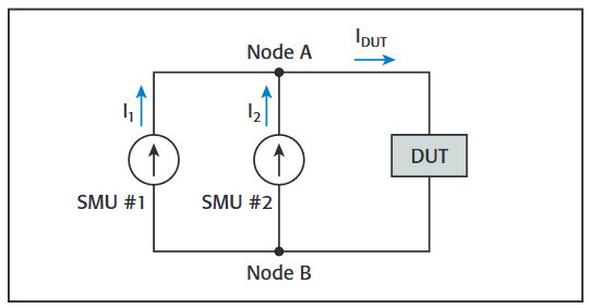
In Figure 2, we can see that two currents, I1 and I2, are entering Node A and a single current, IDUT, is leaving Node A. Based on Kirchhoff's Current Law we know that:
IDUT = I1 + I2
This means that the current delivered to the DUT is equal to the sum of the currents flowing from each SMU. With two SMUs connected in parallel, we can deliver to the DUT twice the amount of current that can be delivered by a single SMU. Using this method with two Model 2651As, we can deliver up to 100A pulsed.
Implementation
In order to create a current source capable of delivering more current than a single SMU can provide, we put two SMUs, both configured as current sources, in parallel. Below is a quick overview of what needs to be done to successfully combine two Model 2651As so that together they can source up to 100A pulsed. The following sections explain each item in detail.
- Use two Model 2651As, running the same version of firmware.
- Use the same current range for both SMUs.
- Use the same regions of the power envelope (Figure 3) for both SMUs.
- Use 4-wire mode on both SMUs with Kelvin connections placed as close to the DUT as possible.
- Use the Keithley supplied cables. If this is not possible, ensure your cabling matches the specifications of the Keithley-supplied cable.
- Set the voltage limit of both SMUs. (When the output of an SMU reaches its voltage limit, it goes into compliance.) The voltage limit of one SMU should be set 10% lower than the other SMU.
- Select the output off-mode of each SMU. This determines whether an SMU will function as a voltage source set to 0V or as a current source set to 0A when the output is turned off. When two SMUs are functioning in parallel as current sources:
- The SMU with the lower voltage limit should have its output off-mode set to NORMAL with the off function set to voltage, and
- The SMU with the higher voltage limit should have its output off-mode set to NORMAL with the off function set to current.
Identical Model
Both SMUs MUST be the same model, the Model 2651A. This ensures that if the SMUs are forced into a condition in which one SMU must sink all of the current from the other SMU, the SMU that is sinking is capable of sinking all the current. For this reason, combining different model SourceMeter instruments in parallel is NOT recommended. In addition, both SMUs should be running the same version of firmware to ensure that both SMUs perform the same.
Source Current Range
Both SMUs should be set to the same source current range. How an SMU responds to a change in current level can vary with the current range on which it is being sourced. By configuring both SMUs to source on the same current range, both SMUs will respond similarly to changes in current levels. This reduces the chances for overshoots, ringing, and other undesired SMU-toSMU interactions.
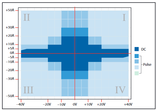
Region of Power Envelope
Both SMUs should be configured to operate in the same region of the power envelope (see Figure 3). In order for one SMU to sink all the current of the other SMU, the sinking SMU must be operating in an equivalent region of the power envelope as the sourcing SMU.
When configured as a current source, the region of the power envelope in which the SMU is operating is determined by the source current range and the voltage limit value. When combining SMUs in parallel, each SMU should be set to the same source current range so the final determining factor for the region is the voltage limit. As can be seen in Figure 3, the Model 2651A has three ranges of voltage limit values that determine the operating region: >0V to ≤10V, >10V to ≤20V, and >20V to ≤40V. For example, if one SMU’s voltage limit is set to 20V, then the other SMU’s voltage limit should be set to a value that is less than 20V and greater than 10V in order to keep both SMUs in the same operating region.
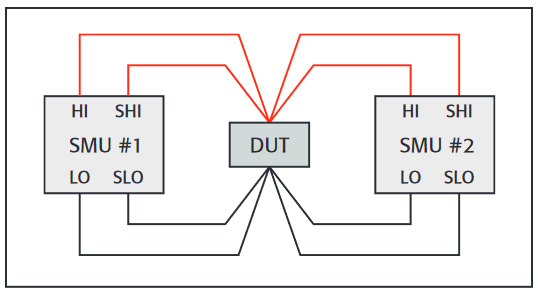
Connections
The fundamental test of a laser diode is a Light-Current-Voltage (LIV) curve, which simultaneously measures the electrical and optical output power characteristics of the device. This test is primarily used to sort laser diodes or weed out bad devices before they can be built into an assembly. The device under test (DUT) is subjected to a current sweep while the forward voltage drop is recorded for each step in the sweep. Simultaneously, instrumentation monitors the optical power output. The resulting data is then analyzed to determine laser characteristics, including lasing threshold current, quantum efficiency, and "kink" detection (localized negative slope in the first derivative optical power output vs. injection current curve).
Cabling Considerations
Cables capable of supporting the high levels of current that the Model 2651A can produce should be used to obtain the desired performance. The cable provided by Keithley with the Model 2651A is designed for both low resistance and low inductance. We recommend using this cable from the Model 2651A to as close to the DUT as possible. If the Keithley cable cannot be used, use wiring with as low a resistance and inductance as possible. We recommend that wire of 12 AWG or thicker be used with a single Model 2651A. When combining SMUs for greater current, 10 AWG or thicker wire should be used. Guidelines for cabling should be taken seriously since wiring not rated for the current being sourced can affect the performance of the SMU and could also create a potential fire hazard.
The following sections discussing resistance and inductance are provided to help you verify that the cables you are using will allow your system to function properly
Resistance
The Model 2651A has the ability to compensate for errors caused by voltage drops due to resistance in the force leads when large currents are flowing. This allows the Model 2651A to deliver or measure the proper voltage at the DUT rather than at the output of the instrument. This is done by using Kelvin connections.
The resistance of any cabling and connections between the SMUs output and the DUT should be kept as low as possible to avoid excessive voltage drops across the force leads. This is because there is a limit to how large a voltage drop an SMU is capable of compensating for without adversely affecting performance. In the Keithley Model 2651A, this limit is 3V per source lead, which is imposed by the Kelvin connections.
A single Model 2651A is capable of sourcing up to 50A pulsed and up to 20A DC. Using Ohm's Law we can calculate the maximum resistance allowed in our test leads so as not to exceed the 3V limit under these maximum conditions. Ohm's Law states:
V = I · R
where: V is voltage, I is current, and R is resistance. If we rewrite this equation, solving for R we get:
R = V/I
To find the maximum resistance values allowed in our test leads, we can substitute our limits for V and I.
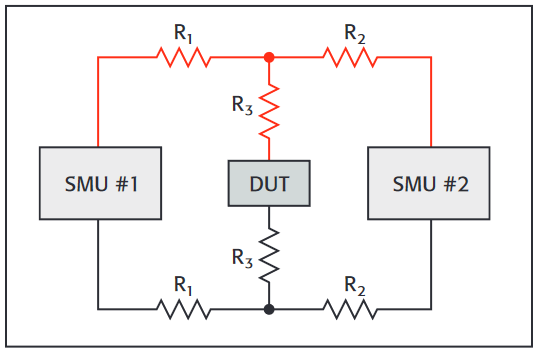
le in order to minimize its resistance value (and thus the voltage drop across R3). In this configuration, the current that flows through R3 is the sum of the current flowing through R1 and R2. If we assume R1 = R2 = R3 and that both SMU #1 and SMU #2 are delivering the same amount of current to the circuit, then the voltage drop across R3 is twice as large as the voltage drop across R1 or R2 because twice as much current is flowing through R3 as there is through R1 or R2. The voltage drop that each SMU sees is the sum of the voltage drop across R3 and the voltage drop across its own lead resistance, R1 or R2
Based on these calculations, the resistance of each source lead should not exceed 150mW when only DC testing is used and should not exceed 60mW when pulse testing is used.
For example, in Figure 5 the length of the test lead represented by R3 should be as short as possible in order to minimize its resistance value (and thus the voltage drop across R3). In this configuration, the current that flows through R3 is the sum of the current flowing through R1 and R2. If we assume R1 = R2 = R3 and that both SMU #1 and SMU #2 are delivering the same amount of current to the circuit, then the voltage drop across R3 is twice as large as the voltage drop across R1 or R2 because twice as much current is flowing through R3 as there is through R1 or R2. The voltage drop that each SMU sees is the sum of the voltage drop across R3 and the voltage drop across its own lead resistance, R1 or R2
Inductance
The Model 2651A also has the ability to compensate for errors caused by voltage drops due to inductance in the force leads. As mentioned in the discussion about resistance, this allows the Model 2651A to deliver or measure the proper voltage at the DUT rather than at the output of the instrument. Inductance in connections resists changes in current and tries to hold back the current by creating a voltage drop. This is similar to resistance in the leads. However, inductance only plays a role while the current is changing, whereas resistance plays a role even when current is steady.
The inductance of connections between the SMUs outputs and the DUT should be kept as low as possible to minimize impacting SMU performance. To drive fast rising pulses, the Model 2651A must have enough voltage overhead to compensate for the voltage drop created by the inductance. If the supply does not have enough overhead, the inductance can slow the rise time of the pulse.
Another reason why the inductance of connections between the SMUs outputs and the DUT should be kept as low as possible is that if the inductance causes a voltage drop large enough to exceed the 3V source-sense lead drop limit of the Kelvin connections, readings could be affected. If the 3V limit is exceeded, readings taken during the rising or falling edge of the pulse could be invalid. However, readings taken during the stable part of the pulse will not be affected.
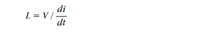
On the Model 2651A, the amount of overhead in the power supply varies depending on the operating region in the power envelope (see Model 2651A datasheet at www.keithley.com/data?asset=55786 for more detail); but, in general, the amount of voltage drop caused by inductance should be kept under the 3V source-sense lead drop limit of the Kelvin connections. We can calculate the maximum amount of inductance allowed in our connections by using the equation:

where: V is the voltage in volts, L is the inductance in henries, and di/dt is the change in current over the change in time. If we rewrite the equation solving for L we get:
As an example, let’s assume that with zero inductance the Model 2651A produces a 50A pulse through our DUT with a rise time of 35µs. In order to not exceed the 3V limit while maintaining this rise time, the max amount of inductance per test lead is:

In this example (35µs rise time for a 50A pulse), to not exceed the 3V limit we must ensure that our test leads have less than 2.1µH of inductance per lead.
NOTE: The Model 2651A specifications indicate a maximum inductive load of 3µH, thus the total inductance for both HI and LO leads must be less than 3µH under all conditions.
Set the Compliance
In parallel configurations, like the one shown in Figure 5, the voltage limit of one SMU should be set 10% lower than the voltage limit of the other SMU. This allows only one SMU to go into compliance and become a voltage source.
Definition
An SMU, or any real current source for that matter, has a limit as to how much voltage it can output in order to deliver the desired current. When the voltage limit in an SMU is reached, the SMU goes into compliance and becomes a voltage source set to that voltage limit. When the compliance on one SMU is set lower than the compliance on the other SMU, the voltage limit can only be reached by one of the SMUs. In other words, when the SMU with the lower voltage limit goes into compliance, it becomes a voltage source with low impedance and begins to sink the current from the other SMU. With the SMU in compliance sinking current, the other SMU can now source its programmed current level and thus never go into compliance.
Setting Correct Voltage Limits
In a parallel SMU configuration, setting voltage limits properly is important. If both SMUs were to go into compliance and become voltage sources, then we would have two voltage sources in parallel. If this condition occurs, an uncontrolled amount of current could flow between the SMUs, possibly causing unexpected results and/or damage to the DUT. This condition can also occur if the DUT becomes disconnected from the test circuit. Fortunately, this condition can easily be avoided by setting the compliance for one of the SMUs lower than the compliance of the other SMU.
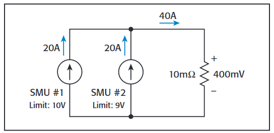
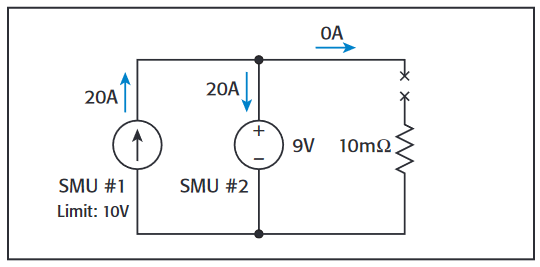
For example, in Figure 6 we have two Model 2651As configured as 20A current sources that are connected in parallel to create a 40A current source. The voltage limit of SMU #1 is configured to 10V and the voltage limit of SMU #2 is configured to 9V and they are sourcing into a 10mW load. If one of the leads disconnects from the DUT during the test, each SMU would ramp up its output voltage trying to force 20A until SMU #2 reaches its voltage limit of 9V and goes into compliance. SMU #1 continues to raise its output voltage until 20A are flowing from it into SMU #2. This condition can be seen in Figure 7. Because the SMUs are the same model, SMU #2 can sink the 20A current SMU #1 is delivering to it. Note that operating in this condition will cause SMU #2 to heat up quickly and will cause it to shut off if it heats up too much. This over-temperature protection is a safety feature built into the Model 2651A to help prevent accidental damage to the unit.
Set the Output Off-Mode
Introduced with the Model 2651A are new features to the NORMAL output off-mode of Series 2600A instruments. Previously, under the NORMAL output off-mode, when the output was turned off, the SMU was reconfigured as a voltage source set to 0V. This would happen whether the SMU’s on state was configured as a current source or a voltage source. This is still the default configuration for the NORMAL output off-mode; however, the NORMAL output off-mode can now have its off function configured as a current source. With the off function set to current, when the output is turned off the SMU is reconfigured as a 0A current source. This happens whether the SMU's on state was configured as a current or voltage source.
When putting two SMUs configured as current sources in parallel, the SMU whose On State voltage limit is set lower should be configured using an output off-mode of NORMAL with an off function of voltage and its Off State current limit should be set to 1mA. The other SMU, whose On State voltage limit is higher, should be configured using an output off-mode of NORMAL with an off function of current and its Off State voltage limit should be set to 40V. To illustrate this, let’s use Figure 6 as an example. For this configuration, both SMU’s output off-mode should be set to NORMAL. Also, SMU #1 should have its off function set to current with an off limit of 40V and SMU #2 should have its off function set to voltage with an off limit of 1mA. (The 40V and 1mA off limits are provided in the configuration guidelines in the reference manual of the Model 2651A.)
Setup of this new output off mode configuration is done through two new ICL commands:
smua.source.offfunc
smua.source.offlimitv
smua.source.offfuncis used to select the off function, for example:
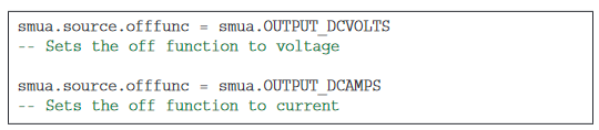
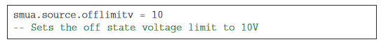
smua.source.offlimitvis used to set the voltage limit of the Off State configuration when the off function is current. It is similar to the command smua.source.offlimiti,which sets the current limit for the off state when the off function is voltage. Example usage follows:
Correctly Setting the Output Off-Mode
If you configure an SMU as a current source and do not change the off-mode, then when you turn the output off, the SMU will switch its source function from current to voltage and begin sourcing 0V. If you did not anticipate this switch, you could have a problem as the SMU essentially becomes a short to whatever is connected to it. If you had two SMUs in parallel and the SMU whose output was still on was operating as a voltage source when the other SMU's output was turned off, you would have two voltage sources in parallel, which could result in excessive current flow and could potentially damage the SMU.
Figure 7 shows what would happen if a connection to the DUT were severed. SMU #2, whose voltage limit is lower, would go into compliance and SMU #1, with a higher voltage limit, would deliver all of its current to SMU #2. If SMU #1’s output were to be shut off unexpectedly and its output mode turned it into a 0V voltage source, then we would have a 0V voltage source in parallel with a 9V voltage source. In this case, SMU #2 would come out of compliance and switch back to a current source. However, uncontrolled current may flow before this switch occurs.
If SMU #1 had its output off function configured as a current source, the unexpected shut off of SMU #1's output would not have resulted in two voltage sources in parallel. Instead, SMU #1 would have simply dropped to a 0A current source. Because SMU #1's voltage limit was set higher than SMU #2's voltage limit, SMU #2 would remain in compliance but now no current would flow in the system since SMU #1 is still in control and forcing 0A.
If the opposite situation were to occur and SMU #2's output turned off unexpectedly, the situation would still be safe. SMU #2, whose off function was configured as a voltage source, would simply drop down from the 9V state to 0V. This is not a problem as SMU #1 is still a current source and holds the current to the 20A it was sourcing. The system is still not settled, however, since SMU #2 is configured with an off limit of 1mA. Because of this, SMU #2 goes into compliance, becomes a 1mA current source, and begins to raise its output voltage to try to limit current to 1mA. At this state, we have two current sources in parallel. As SMU #2 continues to ramp its output voltage, SMU #1 goes into compliance at 10V and becomes a 10V voltage source. In this state, SMU #2, a current source at this time, is in control and only 1mA of current is flowing.
Example
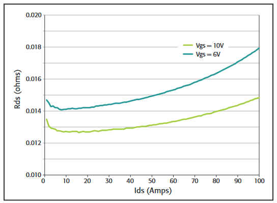
This example is designed to collect Rds(on) measurement data from a power MOSFET device by using a pulsed current sweep to test up to 100A, however, it can be easily modified for use in other applications.
Required Equipment
This example requires the following equipment:
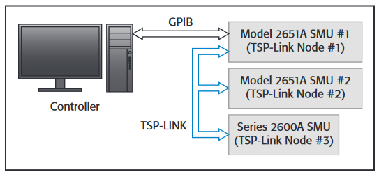
- Two Model 2651A High Power System SourceMeter Instruments that will be connected in parallel to source up to 100A pulsed through the drain of the DUT
- One Model 26xxA System SourceMeter Instrument to control the gate of the DUT
- Two TSP-Link® cables for communications and precision timing between instruments
- One GPIB cable or one Ethernet cable to connect the instruments to a computer
Communications Setup
The communication setup is illustrated in Figure 9. GPIB is being used to communicate with the PC, but this application can be run using any of the supported communication interfaces. The TSP-Link connection enables communication between the instruments, precision timing, and tight channel synchronization.
To configure the TSP-Link communication interface, each instrument must have a unique TSP-Link node number. Configure the node number of Model 2651A #1 to 1, Model 2651A #2 to 2, and Model 26xxA to 3.
To set the TSP-Link node number using the front panel interface of either instrument:
- Press MENU.
- Select TSPLink.
- Select NODE.
- Use the navigation wheel to adjust the node number.
- Press ENTER to save the TSP-Link node number.
On Model 2651A #1, perform a TSP-Link reset to alert Model 2651A #1 to the presence of Model 2651A #2 and Model 26xxA:
NOTE: You can also perform a TSP-Link reset from the remote command interface by sending tsplink.reset() to Model 2651A #1.
- Press MENU.
- Select TSPLink.
- Select RESET.
NOTE: If error 1205 is generated during the TSP-Link reset, ensure that Model 2651A #2 and Model 26xxA have unique TSP-Link node numbers.
Device Connections
Connections from the SourceMeter instruments to the DUT can be seen in Figure 10. Proper care should be taken to ensure good contact through all connections.
NOTE: For best results, all connections should be left floating and no connections should be tied to ground. Also, all connections should be made as close to the device as possible to minimize errors caused by voltage drops between the DUT and the points in which the test leads are connected.
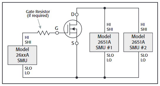
NOTE: During high current pulsing, the gate of your DUT may begin to oscillate, creating an unstable voltage on the gate and thus unstable current through the drain. To dampen these oscillations and stabilize the gate, a resistor can be inserted between the gate of the device and the Force and Sense Hi leads of the Model 26xxA. If the gate remains unstable after inserting a dampening resistor, enable High-C mode on the Model 26xxA (leaving the dampening resistor in place)
Configuring the Trigger Model
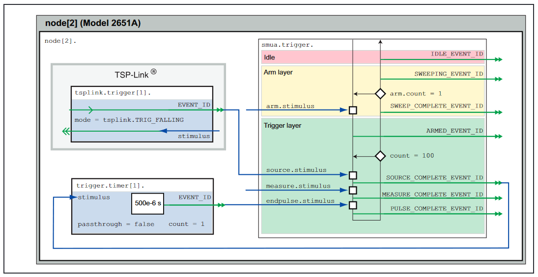
In order to achieve tight timing and 100A pulses with two Model 2651As, the advanced trigger model must be used. Using the trigger model, we can keep the 50A pulses of the two Model 2651As synchronized to within 500ns to provide a single 100A pulse. Figure 11 illustrates the complete trigger model used in this example.
In this example, Model 2651A #1 is configured to control the overall timing of the sweep while Model 2651A #2 is configured to wait for signals from Model 2651A #1 before it can generate a pulse. The Model 26xxA is controlled by script in this example, so its trigger model is not used.
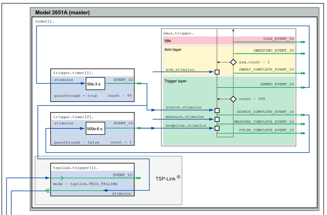
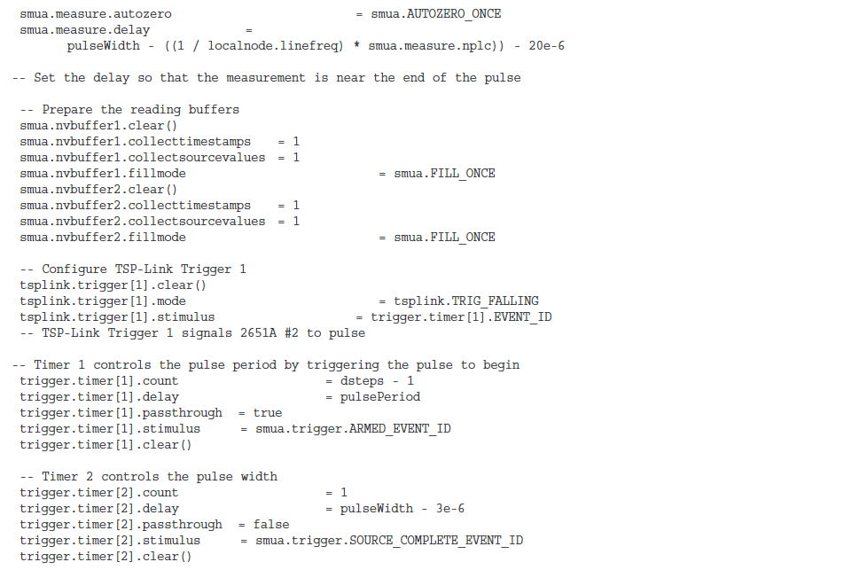
Model 2651A #1 Trigger Model Operation
In Model 2651A #1's trigger model (Figure 12), Timer 1 is used to control the period of the pulse while Timer 2 is used to control the pulse width. TSP-Link Trigger 1 is used to tell Model 2651A #2 to output its pulse.
When the trigger model of Model 2651A #1 is initialized, the following occurs:
- The SMU's trigger model leaves the Idle state, flows through the Arm Layer, enters the Trigger Layer, outputs the ARMED event trigger, and then reaches the Source Event where it waits for an event trigger.
- The ARMED event trigger is received by Timer 1, which begins its countdown and passes the trigger through to be received by TSP-Link Trigger 1, and the SMU's Source Event.
- TSP-Link Trigger 1 receives the event trigger from Timer 1 and sends a trigger through the TSP-Link to Model 2651A #2 to instruct it to output the pulse.
- The SMU's Source Event receives the event trigger from Timer 1, begins to output the pulse, waits the programmed source delay, if any, outputs the SOURCE_COMPLETE event to Timer 2, and then lets the SMU's trigger model continue.
- Timer 2 receives the SOURCE_COMPLETE event trigger from Timer 1 and begins to count down.
- The SMU's trigger model continues to the Measure Event where it waits a programmed measure delay, if any, takes a measurement, and then continues until it hits the End Pulse Event where it waits for an event trigger.
- Timer 2's countdown expires and Timer 2 outputs an event trigger to the SMU's End Pulse Event.
- The SMU's End Pulse Event receives the event trigger from Timer 2, outputs the falling edge of the pulse, then lets the SMU's trigger model continue.
- The SMU's trigger model then compares the current Trigger Layer loop iteration with the trigger count.
- If the current iteration is less than the trigger count, then the trigger layer repeats and the SMU's trigger model reaches Source Event where it waits for another trigger from Timer 1. Because Timer 1 had its count set to the trigger count minus one, Timer 1 will continue to output a trigger for each iteration of the Trigger Layer loop. The trigger model then repeats from Step 3.
- If the current iteration is equal to the trigger count, then the SMU's trigger model exits the Trigger Layer, passes through the Arm Layer, and returns to the Idle state.
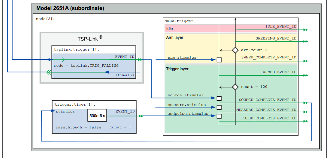
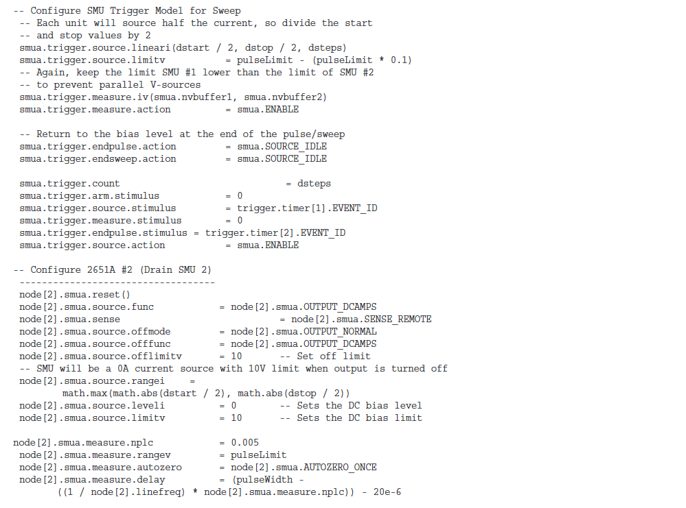
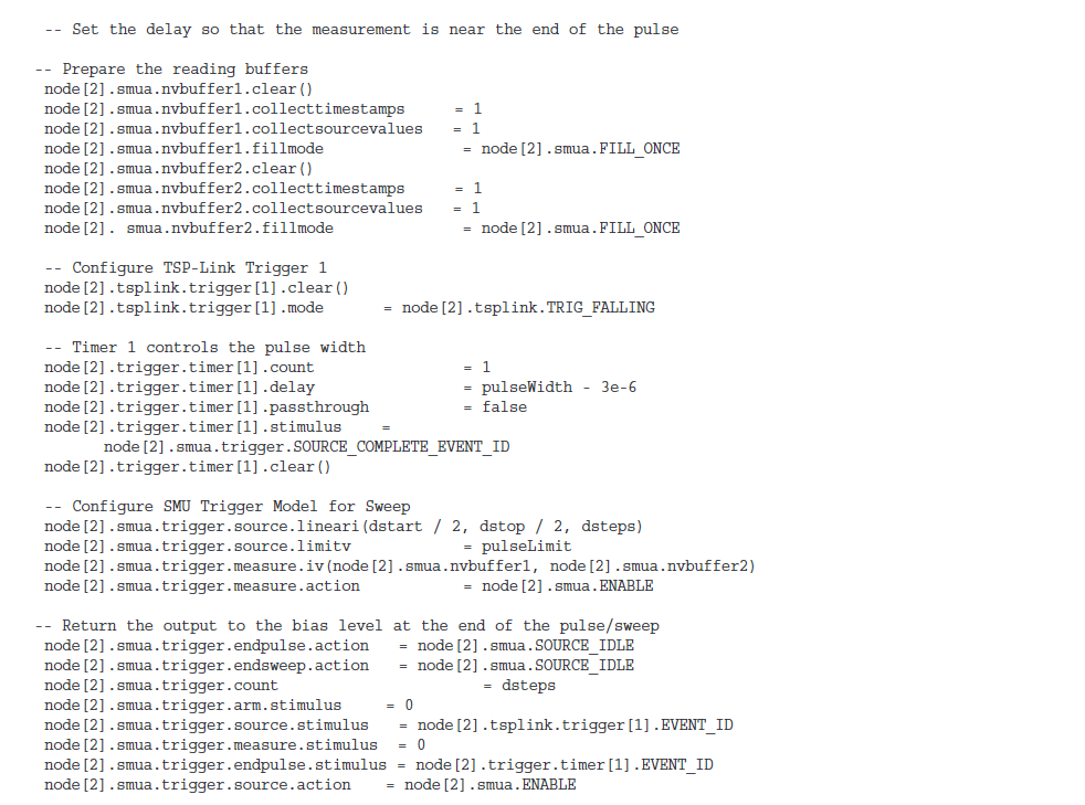
Model 2651A #2 Trigger Model Operation
In Model 2651A #2's trigger model (Figure 13), Timer 1 is used to control the pulse width and is programmed with the same delay as Model 2651A #1's Timer 2. The pulse period is controlled by TSP-Link Trigger 1, which receives its triggers from Model 2651A #1's Timer 1, thus the pulse period for Model 2651A #2 is controlled by the same timer as the Model 2651A #1.
When the trigger model of Model 2651A #2 is initialized, the following occurs:
- The SMU's trigger model leaves the Idle state, flows through the Arm Layer, enters the Trigger Layer, and then reaches the Source Event where it waits for an event trigger.
- TSP-Link Trigger 1 receives a trigger from TSP-Link and outputs an event trigger to the SMU’s Source Event.
- The SMU's Source Event receives the event trigger from TSP-Link Trigger 1, begins to output the pulse, waits for a programmed source delay, if any, outputs the SOURCE_ COMPLETE event to Timer 1, and then lets the SMU's trigger model continue.
- Timer 1 receives the SOURCE_COMPLETE event trigger from TSP-Link Trigger 1 and begins its countdown.
- The SMU's trigger model continues until it reaches the Measure Event where it waits for a programmed measure delay, if any, takes a measurement, and then continues until it hits the End Pulse Event where it stops and waits for an event trigger.
- Timer 1's countdown expires and Timer 1 outputs an event trigger to the SMU's End Pulse Event.
- The SMU's End Pulse Event receives the event trigger from Timer 1, outputs the falling edge of the pulse, then lets the SMU's trigger model continue.
- The SMU's trigger model compares the current Trigger Layer loop iteration with the trigger count.
- If the current iteration is less than the trigger count, then the trigger layer repeats and the SMU's trigger model reaches Source Event where it waits for another trigger from TSP-Link Trigger 1. The trigger model then repeats from Step 2.
- If the current iteration is equal to the trigger count, then the SMU's trigger model exits the Trigger Layer, passes through the Arm Layer, and returns to the Idle state.
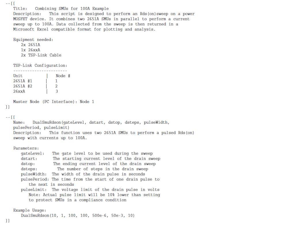
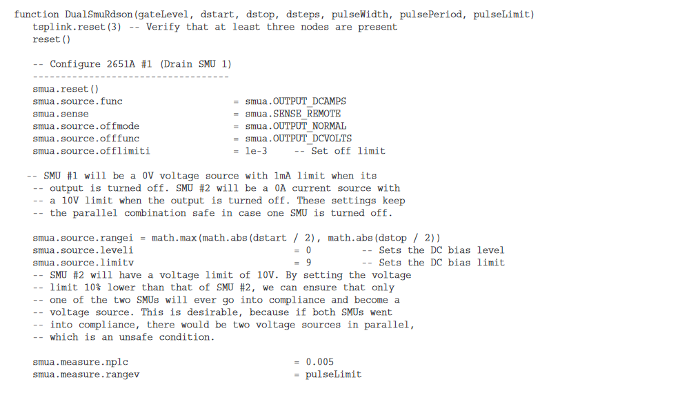
Example Program Code
NOTE: The example code is designed to be run from Test Script Builder or TSB Embedded. It can be run from other programming environments such as Microsoft® Visual Studio or National Instruments LabVIEW®, however, modifications may be required.
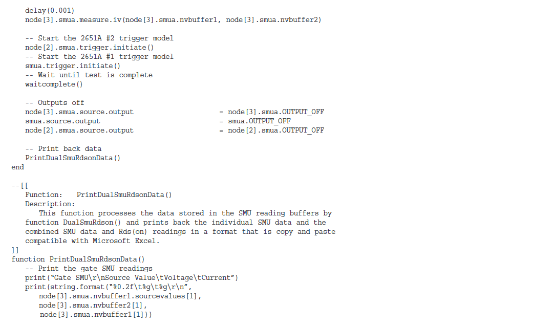
The TSP script for this example contains all the code necessary to perform a pulsed Rds(on) sweep up to 100A using two Model 2651A High Power System SourceMeter instruments and a Model 26xxA System SourceMeter instrument. This script can also be downloaded from Keithley's website at www.keithley.com/base_download?dassetid=55808.
The script performs the following functions:
- Initializes the TSP-Link connection
- Configures all the SMUs
- Configures the trigger models of the two Model 2651As
- Prepares the readings buffers
- Initializes the sweep
- Processes and returns the collected data in a format that can be copied and pasted directly into Microsoft Excel®
The script is written using TSP functions rather than a single block of inline code. TSP functions are similar to functions in other programming languages such as C or Visual Basic and must be called before the code contained in them is executed. Because of this, running the script alone will not execute the test. To execute the test, run the script to load the functions into Test Script memory and then call the functions. Refer to the documentation for Test Script Builder or TSB Embedded for directions on how to run scripts and enter commands using the instrument console.
Within the script, you will find several comments describing what is being performed by the lines of code as well as documentation for the functions contained in the script. Lines starting with
node[2].
are commands that are being sent to Model 2651A #2 through the TSP-Link interface. Lines starting with
node[3].
are commands that are being sent to the Model 26xxA through the TSP-Link interface. All other commands are executed on the Model 2651A #1.
Example Program Usage
The functions in this script are designed such that the sweep parameters of the test can be adjusted without needing to rewrite and re-run the script. A test can be executed by calling the function
DualSmuRdson()
with the appropriate values passed in its parameters.
This is an example call to function
DualSmuRdson()
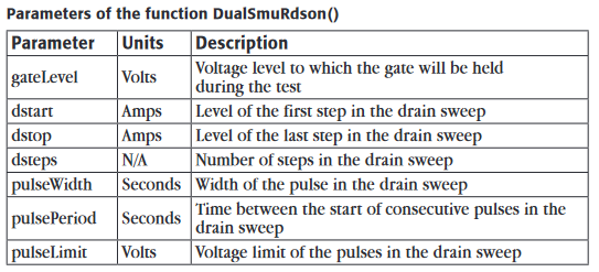
DualSmuRdson(10, 1, 100, 100, 500e-6, 50e-3, 10)
This call sets the gate SMU output to 10V, then sweeps the drain of the DUT from 1A to 100A in 100 points. The points of this sweep will be gathered using pulsed measurements with a pulse width of 500µs and a pulse period of 50ms for a 1% duty cycle. These pulses are limited to a maximum voltage of 10V. At the completion of this sweep, all SMU outputs will be turned off and the resulting data from this test will be returned in an Excel compatible format for graphing and analysis.
Example Test Script Processor (TSP®) Script

Find more valuable resources at TEK.COM
Copyright © Tektronix. All rights reserved. Tektronix products are covered by U.S. and foreign patents, issued and pending. Information in this publication supersedes that in all previously published material. Specification and price change privileges reserved. TEKTRONIX and TEK are registered trademarks of Tektronix, Inc. All other trade names referenced are the service marks, trademarks or registered trademarks of their respective companies.
No.3115 04.19.11