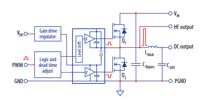
The increase in switching speed offered by GaN transistors requires good measurement technology, as well as good techniques to capture important details of high-speed waveforms. This application note focuses on how to leverage the measurement equipment for the user's requirement and measurement techniques to accurately evaluate high performance GaN transistors. The application note also evaluates high bandwidth differential probes for use with non-groundreferenced waveforms. In order to demonstrate measurement techniques and requirements for the wide ranging families of EPC eGaN® FETs; a (i) high speed, 10 MHz switching frequency, 65 V eGaN FET EPC8009 (Q1 and Q2 in figure 1) based half-bridge board, and a (ii) lower speed, 500 kHz switching frequency, EPC9080 half-bridge demonstration board which uses the 100 V eGaN FET EPC2045 as the top switch (Q1) and 100 V EPC2022 as the bottom switch (Q2) are used. Both boards are configured to operate as buck converters in figure 1.
Impact of Bandwidth on Measurement
The highest bandwidth available from the combined scope and probe system is given by[1]:
where BW-3dB, BW-3dB, Scope, and BW-3dB, Probe are the bandwidths (in Hz) corresponding to the system, scope, and probe, respectively. For this application note, a 2 GHz oscilloscope (Tektronix MSO 5204) is used. The passive probe (Tektronix TPP1000) offers a maximum bandwidth of 1 GHz. The lower value between the scope and probe bandwidths has the greater effect on system bandwidth. In this example, the overall system bandwidth is calculated to be approximately 1 GHz.
When evaluating the layout of PCB (Printed Circuit Board) designs, typical measurements include rise and fall times, peak overshoot, undershoot and the expected switch node rising edge ringing frequency, which can be estimated by using the ringing frequency equation:

In equation 2, LLoop is the high-frequency loop inductance, which is comprised of the high frequency decoupling capacitors, the eGaN FETs (Q1 and Q2), and the PCB connections of the components. Co2 = Coss + Cpar, includes Coss, which is the output capacitance of the bottom side FET Q2 at the Q2 blocking voltage and Cpar is the parasitic and probe capacitance at the switch node. LLoop is estimated to be approximately 200-300 pH for the demo boards considered in this application note [2]. Coss is 30 pF for the EPC8009 in the test voltage range [3], and Cpar is roughly about 10 pF for this demonstration board. This translates to a ringing frequency fr1~1.6 GHz. For the larger capacitance EPC2045 and EPC2022 based design, the ringing frequency is estimated to be fr2~ 0.44 GHz.
It is clear from (1) that the highest system bandwidth available to us is below the ringing frequency of the EPC8009 based design. We will now observe how choice of system bandwidth affects the capture of the switch node waveform for higher speed GaN transistors, such as the EPC8009, and relatively slower switching GaN transistors, such as the EPC2045 and EPC2022. To understand how this works, consider the frequency response of the system plotted in figure 2 below, with the various available measurement system bandwidths, and the ringing frequencies of the two designs considered in this application note.
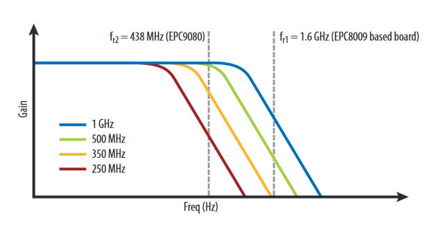
The deeper in the roll-off region fr lies, the less accurate the waveform capture will be for that particular probe. In this case, the measurement system is acting like a low-pass filter, attenuating the high frequency content. This is demonstrated in figure 3, where the waveforms correspond to the colors used in the frequency response shown in figure 2. The difference in the waveforms is evident for the different bandwidth measurements. It is also observed in figure 3 that the rise times of the captured waveforms vary significantly. This can be attributed to the relationship between the system bandwidth and the rise time according to the following equation [1]:
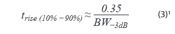
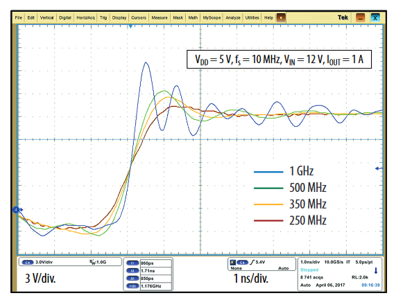
The fastest rise time captured in figure 3 is roughly 0.4 ns, which corresponds to a system bandwidth of ~1 GHz. Using the same probe and oscilloscope with the 500 MHz bandwidth digital filter, the measured rise time is 0.8 ns. Clearly the rise time of the measured signal is limited by the system bandwidth. Since the measured rise time is equal to the calculated system rise time, the input signal is faster than the measurement system rise time. Therefore, the input signal rise time is likely much less than 0.4 ns.
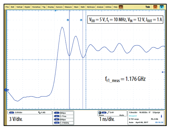
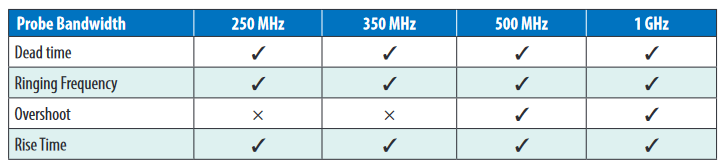
The measured ringing frequency, fr1, is 1.176 GHz as shown in figure 4. This measurement was made with the highest bandwidth 1 GHz probe. The lower bandwidth cases shown in figure 3 further degrade the accuracy of the ringing frequency measurement. When looking at the peak voltage overshoot, it is also clear that lower bandwidth measurements underestimate the peak voltage across the switching devices. For timing dependent dead time measurements, the system bandwidth is also important. Shown in figure 3, there is a more definitive drop in the switching waveform for the bandwidths of 500 MHz and 1 GHz and the dead-times could be more clearly defined from measurement. At lower bandwidths, the drop becomes harder to clearly define. Table 1 shows the system bandwidths impact on the ability to make critical measurements for the highest speed, EPC8009 based board.
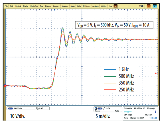
The other test case is shown with the EPC9080 demonstration board, which has a much lower ringing frequency and switching speed from lower on-resistance and higher capacitance eGaN FETs [4]. The corresponding waveforms are shown in figure 5. The ringing frequency (fr2) of 438 MHz and its amplitude measured with the 1 GHz (blue) probe is valid, since fr2 is below the -3dB frequency of the system. The 1 GHz (blue) and 500 MHz (green) waveforms capture all the details accurately. However, for system bandwidths of 350 MHz (orange) and 250 MHz (brown), fr2 is above the system bandwidth. As a result, it captures the ringing waveform shape, but the attenuation on the ringing is evident, thus underestimating the overshoot. The rise time measured by the different system bandwidths are roughly ~ 3 ns. The lowest bandwidth we have used is 250 MHz, which corresponds to a rise time of 1.6 ns according to (2) and for all of the cases the rise time can be captured accurately. This discussion is summarized in table 2.

Measurement Techniques
In the second part of this application note, we demonstrate how good probing techniques and the importance of choice of measurement point in generating a high-fidelity and accurate waveform.
1.Use a probe with low input capacitance and keep ground as short as possible
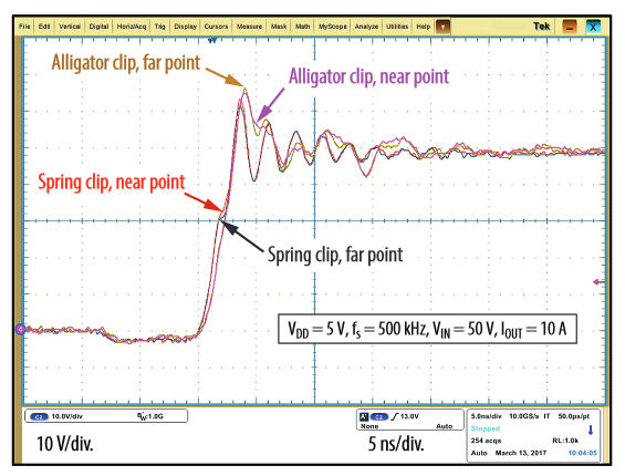
Two types of probe grounding solutions are used for the passive probe (Tektronix TPP1000): An alligator clip and a spring clip [5] (shown in figure 6).
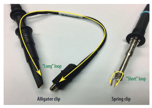
A long ground lead is convenient because the user can make one ground connection and probe many test points within the range of the ground lead. However, any piece of wire has distributed inductance, and the distributed inductance reacts to AC signals by increasingly impeding AC current flow as signal frequency increases. The ground lead's inductance interacts with the probe input capacitance to cause ringing at a certain frequency (see equation 2). This ringing is unavoidable and may be seen as a sinusoid of decaying amplitude. As the length of the ground lead increases, the inductance increases and the measured signal will ring at a lower frequency.
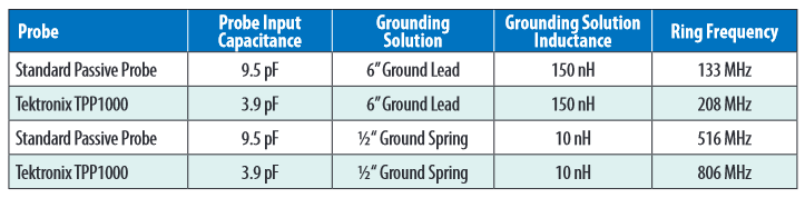
It is important to minimize the effects of the probe's input capacitance and ground lead length. It should be noted that the TPP1000's 3.9 pF input capacitance is significantly lower than other passive probes which have approximately 9.5 pF input capacitance. Table 3 shows how input capacitance and ground lead length affect ringing frequency
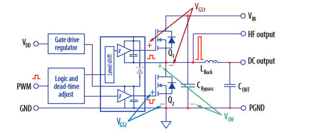
The EPC9080 half-bridge demonstration board will be used as the basis of this section on measurement techniques. Figure 7 shows the schematic of the various test points used in this board, and figure 8 shows a photo of the actual PCB. The switch node waveform is measured at two points as shown in figure 8: a "near point," which is close to the switch node of the FETs, and a "far point," which are the pin headers at the periphery of the PCB.
The waveforms at the switch node (VSW) measured with each combination of probing point and probing technique are shown in figure 9.
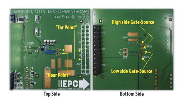
The measured waveforms of figure 9 clearly show that probing technique supersedes the choice of measurement point. Although there is a marginal attenuation, the red and black waveforms are nearly identical. The waveform shape is quite inaccurate when the alligator clip is used, regardless of the choice of measurement point. As a recommendation, the spring clip technique should be used in conjunction with a measurement point which is closest to the power device ("near point").
2. Use an isolated measurement system for nonground referenced high frequency measurements
Differential measurements describe any measurement between two test points but the term is most commonly used when describing measurements involving test points that are not referenced to ground. A few commonly used methods for measuring differential signals are: (a) using two single-ended probes and oscilloscope math to measure the difference, (b) using a high bandwidth, high voltage differential probe, and (c) using an isolated measurement solution [6].
First consider the method of using the math function in the oscilloscope. The voltages at the two test points of interest are measured using two ground referenced probes. Then, a math waveform can be created showing the difference between the two voltage waveforms. The difference math waveform is a pseudo differential measurement. While limited in performance, this technique may be adequate for some low frequency measurements with small common mode signals. For proper operation, both inputs must be set to the same scale factor, and the probes must be identical models and closely matched. Any mismatch between the probe's attenuation/gain, propagation delay and mid and high frequency response will result in less accurate measurements. Common mode rejection ratio (CMRR) is extremely poor at higher frequencies and large common mode signals will overdrive the scope inputs.
The next method for making differential measurements uses a differential probe. Because these probes are truly differential, both of the inputs are high impedance (high resistance and low capacitance). With the balanced, low capacitance inputs of high-voltage differential probes, any point in the circuit can be safely probed with minimal loading to the circuit under test. However, conventional differential probes often fail to provide a good representation of the actual signal due to limitations in their common mode rejection ratio, voltage derating over frequency, frequency response, and the probe's long input leads. These limitations are even more pronounced when testing on power devices with fast switching rates at even nominal common mode voltage.
The most preferred method for making accurate differential measurements are high performance, isolated measurement solutions such as the Tektronix IsoVu measurement system. In circuits such as a half bridge where there are large common mode voltages and fast edge rates, signals such as the high-side gate-source voltage are impossible to measure without superior CMRR at high frequencies. While traditional differential probes offer relatively good common mode rejection at low frequencies up to a few MHz, their CMRR will substantially degrade past a few megahertz. An isolated system such as the Tektronix IsoVu enables high CMRR at high frequencies. When evaluating signals such as a high-side VGS riding on top of the switch node voltage, which is rapidly switching between "ground" and the input supply voltage, a measurement solution with the following characteristics is required:
- Galvanic isolation
- High bandwidth: > 500 MHz
- Large common mode voltage: > the input supply voltage
- Large common mode rejection ratio: > 60 dB at 100 MHz
- Large input impedance: > 10 MΩ || < 2 pF
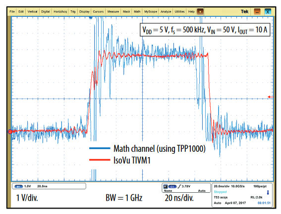
The resultant measurement difference between the scope math technique and an isolated measurement system is illustrated in figures 10 and 11. The waveform that is measured is the highside gate-to-source signal (VGS1) of the EPC9080 board (figures 7 and 8).
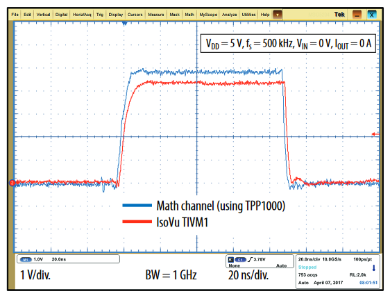
Figure 10 shows the waveforms with only the logic circuits powered in a less noisy or "clean" environment (logic power supply Vdd = 5 V). The passive probe based math waveform is similar to the one measured with high bandwidth isolated probe (Tektronix IsoVu [7]). However, when the circuit is powered with the voltage and current in figure 11, there is a high level of switching noise present in the “noisy” environment magnifying the difference between the measurements. The waveform captured with the isolated probe is much cleaner due to its high CMRR (common mode rejection ratio) [7].
3. A probe's Common Mode Rejection Ratio (CMRR) is a critical, but often overlooked, specification
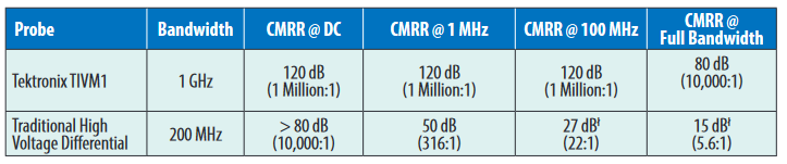
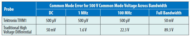
The probe's ability to reject the common mode signal is its common mode rejection ratio (CMRR). Ideally, a differential measurement system would have an infinite CMRR. The higher an amplifier's CMRR, the less impact the common-mode input voltage has on the differential measurement. In practice, a CMRR of at least 80 dB (10,000:1) will result in usable measurements. Most differential probes can easily obtain a CMRR of 80 dB or higher at DC and low frequencies where it's possible to tune the components accurately. As the frequency of the measurement increases, a differential probe's CMRR degrades because the mismatches become increasingly difficult to control. At 100 MHz, the CMRR capability of most measurement systems is 20 dB or less. Table 4 compares the CMRR specifications of an isolated measurement system (Tektronix TIVM1) versus a traditional high voltage differential probe. These values are taken directly out of the probe's data sheets.
Because the CMRR capabilities of a traditional differential probe are only effective from DC to a few megahertz, a typical data sheet fails to provide a CMRR number at higher bandwidths. A user may fall into the trap of thinking the 1 MHz specification is "fast enough" for their application. However, it's important to remember that while the repetition rate may not be fast, the rise time of the signal you're measuring may be quite fast, in the 1's or 10's of ns.
If the differential signal that is being measured is in the presence of 500 V common mode voltage, how much error should you expect? Again, it depends on the signal's rise time. If the measurement is being made at DC using a traditional differential probe, the CMRR is 80 dB or 10,000:1. The common mode error is 500 V divided by 10,000, which is 50 mV of error. Table 5 shows how much common mode error the user would experience in the presence of 500 V common mode voltage across bandwidth.
Note: Because the values at 100 MHz and full bandwidth for traditional probes are not listed in the data sheet, these values were extracted from the common mode rejection plot in the user manual.
Conclusion
Measuring various EPC eGaN FET based power converters, including impacts of bandwidth, probing techniques, and appropriate use of highbandwidth isolated probes has been described in this application note. Combining better measurement technologies and techniques with improved understanding of the requirements of the measurement system for a specific application, circuit designers can better optimize their high performance GaN based designs.