
Свяжитесь с нами
Живой чат с представителями Tektronix. С 9:00 до 17:00 CET
Звонок
Позвоните нам
С 9:00 до 17:00 CET
Загрузить
Загрузить руководства, технические описания, программное обеспечение и т. д.:
Обратная связь
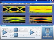
Serial Data Link Analysis Visualizer
Option SDLA64, DPOFL-SDLA64 (Real-Time), and JNB02 (Sampling)
Option SDLA64, DPOFL-SDLA64 (Real-Time), and JNB02 (Sampling)
SDLA Visualizer and DPOJET with simultaneous views of a PCI Express 3.0 acquired signal, signal after compliance channel embedding, CTLE and DFE receiver equalization
Features and benefits
- Complete Measurement Circuit De-embed Environment
- Remove reflections, cross-coupling, and loss caused by fixtures, cables, probes allowing visibility of the true circuit behavior
- Simulation Circuit Embed Tools
- Embed user defined channel models to simulate the signal at the end of the link without needing physical channels
- Receiver Equalization Flexibility
- Open closed eyes caused by channel effects using receiver equalization techniques, such as Continuous Time Linear Equalizer (CTLE), Decision Feedback ( DFE), or Feed Forward (FFE) Equalization
- Model silicon-specific receiver equalization using IBIS-AMI models to observe on-chip behavior
- View the signal at locations that can not be physically probed
- Allows measurements on signals that otherwise have reflections due to non-ideal probe points
- Advanced Analysis and Modeling Capabilities
- Flexible modeling including cascading of 4-port S-parameters (differential and single-ended), 2-port S-parameters, TDT Waveforms, RLC Models, loss-less transmission lines, probes, or FIR filters
- S-parameter and filter scaling to model loss based on a percentage of the actual model
- "What-If" analysis to evaluate the optimal transmitter settings using flexible insertion/removal of transmitter equalization parameters
- Twelve test points allow simulated probing where physical probing is not practical
- View the common mode, differential, or individual inputs of the signal
- Simultaneously view and measure time-aligned waveforms at multiple test points using integrated DPOJET Jitter and Eye Analysis (opt. DJA) support for real-time scopes
- Creation of filters for use with JNB02 on the Tektronix DSA8300 Sampling Oscilloscope
- Automatic measurement of desired test point with JNB for sampling scopes
- Comprehensive frequency and time domain plots, enable quick verification of S-parameters and test point transfer functions
Applications
-
De-embedding the effects of cables, fixtures, and probes for silicon validation
-
Characterization of backplane and embedded system performance using IBIS-AMI CTLE, DFE, or FFE receiver equalization
-
Link budgeting and What-if Analysis with emulation of a range of channels
- Evaluate Transmitter Equalization (De-emphasis/Pre-emphasis)
-
Reflection removal caused by impedance mismatch for high speed serial buses and DDR
-
Characterize the performance for multi-gigabit standards such as SATA, USB 3.0, SAS 12 Gb/s, PCIe Gen 3, OIF CEI, XFP, IEEE 802.3 Ethernet
SDLA Data Link Visualizer overview
Acceleration of signaling speeds and shrinking geometries create several challenges for next generation multi-gigabit designs and test methodologies. Designs are evolving to address these challenges with advanced equalization techniques at the transmitter and receiver. Smaller form factors make signal access more difficult resulting in nonideal probing points. This can lead to loss and reflections on the acquired signal due to impedance discontinuities that are not present at the ideal measurement location.
The advanced techniques employed by the designs call for advanced measurement solutions. The challenge begins with the signal acquisition: capturing a signal through cables, probes and fixtures distort the signal shape; SDLA Visualizer allows you to de-embed the effects (reflections, insertion loss, and cross coupling) of the measurement circuit (cables, probes, and fixtures) from the waveform while taking into account the transmitter output and receiver input impedance. De-embedding these effects improves the accuracy of measurements and can make the difference between passing or failing a test.
After de-embedding the measurement circuit, what-if scenarios can be run by embedding a simulation circuit. This could consist of a simple ideal 50 Ω receiver load for transmitter characterization or could be a simulated channel that represents a backplane.
In many situations, after embedding the simulation circuit the effects of the channel loss result in a closed eye. Many analysis applications provide reference receiver equalizers; however, a limitation with this approach is that the algorithms typically do not match what is happening in real silicon. IBIS-AMI meets this need by allowing silicon vendors to model the actual receiver implementation in a way that does not expose intellectual property. SDLA Visualizer’s equalization features can emulate receiver equalization by applying an IBIS-AMI model, CTLE, FFE, or DFE equalization.
In other cases, the signal under test must be accessed with a high impedance probe, where the probe point is located at a position which results in capturing reflections due to impedance discontinuities that are not present at the test point. These reflections can make it difficult or impossible to measure the system under test. A method to allow simulated probing while removing reflections is needed. Using SDLA, the reflections and any loading caused by the probe can be removed by modeling the system under test and the measurement circuit. This can be done by using S-parameters of the system or by using RLC and transmission line models.
Another challenge results from the transmitter signal shape. The signal is no longer a simple NRZ square-wave pattern. Designers alleviate high-frequency loss in the media with transmitter equalization features; that is, with pre-emphasis or de-emphasis of the transmitter waveform. Correspondingly, transmitter signals today need to be evaluated for this transmitter equalization; the SDLA software allows for complete transmitter equalization insertion or removal.
SDLA Visualizer provides a common link analysis platform for both real-time and sampling oscilloscopes. Due to platform differences, the following SDLA Visualizer features are available on real-time scopes only:
De-Embedding the measurement circuit
SDLA provides the ability to completely remove the insertion loss, reflections, and cross coupling effects caused by the measurement circuit while taking into account the characteristics of the system under test. The transmitter impedance is modeled by either a nominal impedance or two 1-port or one 2-port S-parameter model. The De-Embed block within SDLA allows for the definition of up to 8 block elements that describe the measurement circuit, for example fixtures, cables, and oscilloscope.
Each block can be described as one of the following:
- 4-port S-Parameter
- Two 2-port S-Parameters
- Transfer function
- FIR filter
- TDT Waveform
- RLC model
- Lossless transmission line model
- High impedance probe
Within the De-Embed block there are two test points which allow for visibility within the cascaded network while viewing the signal with the loading of the measurement circuit.
When using high impedance probes with a real-time oscilloscope, a 3-port probe model is necessary to accurately represent the interactions of the probe with the transmitter, receiver, and the oscilloscope. SDLA ships with 3-port probe models for many of the P76xx, P75xx, and P73xx series probes and input impedance models of the DPO/DSA/MSO70K series oscilloscopes.
SDLA De-Embed block with High Impedance Probe De-Embed enabled.
SDLA Visualizer can also de-embed the effects of interposers used for DDR. By using 3-port and 6-port S-parameter files, the effects of the interposer and probe on both the single-ended and differential signals can be removed. This model can also remove the effects of other measurement circuit elements when probes are being used, for example, a RF switch.
Bandwidth control
When de-embedding, it is critical to pay close attention to the signal to noise ratio at higher frequencies. While SDLA can automatically determine the bandwidth limit for the de-embed filter, it is often necessary to fine tune the filter. Some solutions are limited to a simple bandwidth limit control; however, in some cases this may not be enough. For this reason, SDLA Visualizer provides the ability to control the filter rolloff by adjusting the stopband in frequency and in dB. The examples below show how using the fine tuning capability of SDLA, unwanted artifacts due to a simplified de-embed implementation are not present in the resulting signal.

Mask hit violations on a PCIe 5 Gb/s signal without bandwidth fine tuning.

After fine tuning the filter stopband, the mask hits have been eliminated.

SDLA Bandwidth and Stop Band Control.
The eye diagrams above show the results of using the default stopband settings verus fine tuning. Notice that the preshoot on the signal is reduced, eliminating the upper mask violation.
Embedding the simulation circuit
Once the effects of the measurement circuit have been removed, the simulation circuit can be defined to observe the signal without the effects of the measurement circuit. This is easily done in SDLA by defining the transmitter output impedance, which can be defined as a nominal value, two 1-port or one 2-port S-parameter model. The Embed block can then be configured to represent a simple load or a series of cascaded elements such as transmission lines and connectors. Like the De-Embed block, the Embed block allows for the definition of up to 8 cascaded block elements.
Each block can be described as one of the following:
- 4-port S-Parameter
- Two 2-port S-Parameters
- TDT Waveform
- FIR filter
- RLC model
- Lossless transmission line model
- High impedance probe
In addition, SDLA Visualizer can add or remove Transmitter Equalization. SDLA supports adding pre-emphasis, de-emphasis, 3-tap FFE, and can also read a user defined FIR filter.
Applying equalization
Whether using a simulated circuit or capturing the signal at the far end of the link it is often necessary to apply receiver equalization to open the eye before measurements can be performed. In most cases the lack of physical access makes it impossible to verify the receiver circuit behavior and monitor the effects of clock recovery and equalization. SDLA Visualizer provides a rich set of capabilities for RX equalization, including IBIS-AMI support, CTLE, DFE and FFE. Using the built in support for IBIS-AMI provides the advantage of using silicon specific equalization algorithms that provide the greatest level of correlation between what the receiver actually sees and the simulated waveform. When IBIS-AMI models are not available, SDLA Visualizer can be used to perform CTLE, DFE and FFE.

SDLA Visualizer IBIS AMI Receiver Equalizer Configuration (Real Time only).
Complete link visibility
Within SDLA, twelve test points are provided with four moveable test points in the De-Embed and Embed paths, allowing the maximum flexibility to simulate probing the signal at any point within the system. Test Points in the De-Embed path show the signal with all the loading that is included in the measurement circuit, allowing visibility of the signal with the effects of loading from cables and probes. To visualize the signal without the effects of the measurement circuit, any of the test points along the simulation circuit can be observed. When computing the test points, SDLA automatically removes the delay so the embedded or de-embedded waveforms are time aligned. Alternatively, the delay can be preserved by selecting the “keep delay” option in the Test Point Menu as shown above.
When using SDLA Dual Input mode, each leg of the signal is processed independently through the network. In Dual Input mode the common mode, differential, or individual inputs of the signal can be viewed simultaneously. The effects of reflections, transmission lines, and crosstalk are taken into account by using all the S-parameter terms throughout the system to build the test point transfer functions.
Unlike other solutions which provide visibility of a single test point, SDLA Visualizer allows up to four test points plus the data and clock waveforms after DFE to be visible at one time. Together with DPOJET or JNB, jitter and timing properties of the signal at multiple test points can be measured simultaneously enabling quick comparisons and validation of the data.

SDLA Visualizer Test Point Menu with Individual Inputs, Differential and Common Mode Views enabled for a single test point (Differential only for Sampling Oscilloscopes).
Real-time measurements and jitter analysis
Signals processed with SDLA might require multi-UI measurements, jitter breakdown, jitter bathtub analysis, or other evaluation. DPOJET (Option DJA) is recommended for these tasks. SDLA and DPOJET work together to analyze jitter, generate eye diagrams of equalized waveforms and several other views and measurements. Using the Analyze feature of SDLA, DPOJET is automatically configured to plot an eye diagram and TIE measurement for all enabled test points.

Apply and Analyze menu for DPOJET configuration.
Sampling measurements and jitter analysis
Like DPOJET, JNB Jitter Noise and BER analysis (Option JNB02) can be used on the sampling scope to perform jitter and noise breakdown and other measurements. SDLA Visualizer works with the Signal Path function built into JNB Advanced. After configuring SDLA Visualizer, selecting the desired test point, and applying the model, the filter for the selected test point will automatically be loaded into the Signal Path filter block.
If DFE or FFE equalization are required, those parameters can be quickly entered in the JNB Signal Path and then the final measurements can be done.

JNB Advanced Signal Path with Filter, Channel, and Equalizer enabled
JNB features a rich set of measurements which enable the breakdown of the causes of both vertical and horizontal eye closure. The illustration below shows the measured signal after applying a filter, created by SDLA Visualizer, representing a high loss channel and adding DFE equalization to open the eye.

All of the features of SDLA Visualizer are available for use with both sampling and real-time scopes, with the following exceptions that are available on real-time scopes only: Dual Waveform Input, Filter Keep Delay, Filter export for 32-bit scopes, High Impedance Probe De-Embed, Receiver optimization for PCI Express 3.0, MIPI, and USB 3.1, IBIS-AMI, and DFE (DFE for sampling is done using JNB02 Signal Path).
Plot of elements of the system
In many situations, the information about channels, fixtures, or cables, represented by an S-parameter touchstone file or other information about the system is not completely clear. A supplier might have, for example, supplied you with a touchstone file without properly labeling its ports. To resolve the port assignment and in general to present a view of network response, SDLA offers plots for each block in the De-Embed and Embed path. Both time and frequency domain plots of all 16 S-parameters elements are provided. Overlay plots of the 16 S-parameters allow for quick correlation between different elements for example to compare s21 and s12 to verify equivalence.
Plot types include:
- Magnitude vs. Frequency
- Phase vs. Frequency
- Impedance as a function of frequency
- Smith Chart
- Step Response
- Impulse Response
Plots are available for each block in the De-embed and Embed blocks with Magnitude, Impulse Response, Step Response, and Phase plots for each test point.

Smith Chart allows analysis of the reflection coefficients plotted as impedance for each block in the Embed and De-embed paths.

Full S-Parameter plot.
Practical applications of SDLA Visualizer
Cable de-embedding
Many next generation serial standards require the de-embedding of cables and fixtures that are used to access the device under test. With SDLA Visualizer, the effects of the cables and fixtures can be easily removed by modeling using the De-Embed block. For differential systems a cable pair is often used to attach to the device under test. In many cases each side of the cable is modeled as a 2-port S-Parameter file. SDLA Visualizer allows you to easily specify each side of the cable as separate 2-port S-parameter files. When using SDLA dual input mode, each test point in SDLA can then be represented as the common mode, differential, or individual inputs of the signal allowing for the maximum flexibility in viewing the test point. Processing and viewing the individual inputs of the signal allows differences in each input to be observed and analyzed quickly.

SDLA Visualizer Dual Input mode showing individual inputs of the raw waveform and after de-embedding to remove reflections.
Virtual probing
As form factors become smaller and smaller, the ability to probe the device under test at the desired test points becomes challenging. The resulting signal at the probe point often has reflections that are not present at the ideal test point. These artifacts make it difficult or even impossible to measure the signal. With SDLA Visualizer, the user is able to probe where they can and measure where they need. In the example below, SDLA Visualizer was used to remove reflections from a DDR signal by approximating the receiver impedance, the transmission line delay between the probe point and the receiver, and by specifying the package model of the receiver. Once the virtual probe location is established, the signal can be measured using DDR Memory Bus and Electrical Validation Software (DDRA).
Channel simulation
An important part of today’s evaluation of serial data links is the interaction between the measured waveform and the complex behavior of the interconnect channel. It is no longer possible to assume that if the transmitter output meets the eye diagram mask, a design will work against all channels up to a given loss. Instead, advanced link test methods need to acquire the true transmitter waveform, then test against several corner-case channels.
In some cases this test can be performed with real physical channels: by connecting the transmitter under test to the suite of normative test channels, one channel at a time. However, this methodology is still prone to errors. Certainly each physical device has tolerances against the standard’s ideal values; furthermore the physical channels may vary making a virtual channel more stable. Since physical corner-case channels are typically not conveniently available, virtual channels based on the network description file, for example S-parameter touchstone files can be used. Now the measurement on your transmitter under test simply involves acquisition of the transmitter signal. Then each channel can be embedded in software rather than using a separate physical connection for each channel model.
SDLA Visualizer supports channel simulation by using the Embed block to model the simulation circuit. Once the measurement circuit is removed from the signal path, the channel model can be quickly entered into SDLA to characterize what-if scenarios. For those cases where the simulated channel causes a closed eye, SDLA Visualizer receiver equalization can be used to open the eye.

DDR acquired signal shown with reflections and after virtual probing at the input of the receiver with SDLA Visualizer.

SDLA Visualizer with probe de-embed enabled showing all the block element options.
Receiver equalization
Transmitter equalization is one technique used to compensate for loss and dispersion in the interconnect; another technique is the equalization at the receiver. Receiver equalization in most modern NRZ systems falls under either CTLE (Continuous Time Linear Equalization); FFE (Feed Forward Equalization, also known as LFE (Linear Feedback Equalization); or DFE (Decision Feedback Equalization). A receiver equipped with equalization can decode signals which, when viewed as an eye diagram, produces a closed eye. How can measurements be performed on a closed eye?
The equalization tools in the SDLA can open even a completely closed eye, with your own equalizer tap values; or, at a push of a button, optimized equalization tap values are found for you, even on random data. The speed of recalculation and the ease of use allow you to easily modify system parameters, such as the number and weight of taps, or the amount of pre- or de-emphasis; you can optimize the design, develop what-if scenarios, or confirm your simulations over a range of conditions.
PCI Express 3.0, for example, requires a specific equalization scheme which optimizes a CTLE and one tap DFE. SDLA Visualizer has built in support to find the optimal CTLE setting and DFE tap value to maximize the eye area of the signal as required in the PCI Express 3.0 specification. All the intermediate results are available, which can be used to verify the results against the expected values.
In many cases, it is desired to observe the behavior of a silicon specific equalization model. Since silicon implements proprietary techniques a model of the silicon behavior is required. Many vendors offer IBIS-AMI models that can be used directly in SDLA Visualizer, which provides a truer representation of the signal. When using IBIS-AMI models a complete history of the adaptation record is available. The end results and the adaptation record can be compared with simulation results.
When using the DSA8300 sampling oscilloscope, FFE/DFE can be applied directly in the JNB Signal Path software and CTLE filters can be created using SDLA Visualizer.
Other utilities
SDLA has integrated utilities that provide basic functions for a variety of tasks. In some cases, it may be necessary to normalize each port of an S-parameter model. This can easily be done in SDLA, it is as simple as loading the S-parameter model, assigning the impedance for the ports, and saving the normalized S-parameter model. This is useful when the ports of an S-parameter model may have a different reference impedance than other S-parameter models that are needed to create a model in SDLA.
In other cases, an S-parameter model may have a dip at a certain frequency. This can cause issues when de-embedding due to the extreme boosting of the dip. In some cases these dips may not cause an issue for the actual receiver and it is desired to smooth the resulting filter over a specified frequency range.
SDLA also has a built in utility to re-sample S-parameter models to ensure that they are evenly spaced for use. The utility comes complete with plots, which allow you to verify the results by overlaying the original and the re-sampled S-parameter model. While the frequency spacing is pre-determined, this can also be tuned by the user.
Lastly, while SDLA supports 4-port modeling it is often the case that S-parameter files are generated with 6, 8, 12, or 16 ports. These S-parameter models can be directly entered into SDLA, the user then selects the 4 ports of interest for analysis.
Network measurement tools
Whenever S-parameters of the network are needed, SDLA will accept data from either VNA or a TDR-base S-parameter measurement system. It is recommended that the frequency spacing of the S-parameter data is evenly spaced, however, SDLA also provides a utility that can be used to convert unevenly spaced S-parameters. The utility provides both frequency and time domain plots so the conversion can be verified against the original S-parameter. We recommend Tektronix TDR hardware and Tektronix IConnect® software for high-quality network measurements. Among the advantages of using Tektronix TDR and IConnect is the preservation of the DC values in the Touchstone matrix, which is typically lost with other measurement methods. SDLA accepts network description based on other measurement methods, such as VNA data or field-solver calculation; the DC measurement results might need to be extrapolated. SDLA will extrapolate the data to DC in these cases.
Additional information
For additional information, we recommend the following resources: literature on the DPO/DSA/MSO70000 Series oscilloscopes, their probes and software applications; literature on Tektronix TDR/TDT and the IConnect network measurement software; and literature on the DSA8300 Series sampling oscilloscope and software applications.
Specifications
- Transmitter impedance
-
Nominal, two 1-port, or 2-port Touchstone S-parameter matrix, with selectable port assignments.
- Transmitter equalization
-
3-tap FFE, UI-spaced, or a custom FIR filter of 12000 taps max. Configurable as either pre-emphasis or de-emphasis, insertion or removal.
- Receiver impedance
-
Nominal, two 1-port, or 2-port Touchstone S-parameter matrix, with selectable port assignments
- Receiver equalization type
-
CTLE: 2nd-order IIR filter, or a custom FIR filter of 12000 taps max. FFE, up to 100 taps, settable pre/post-cursor, whole UI or fractional spacing. DFE, up to 40 taps. Taps can be set or trained. (FFE and DFE Real-Time only. Sampling DFE supported with JNB02 Signal Path).
- Receiver equalization training
-
Vertical Noise targeting algorithm. Random data acceptable for training; repetitive pattern recommended for training of highly distorted data. Pattern detection and export/import. Training from unspecified tap values or adaptive from previously found or loaded values. (Real-Time only)
- PCI Express, USB 3.1, and MIPI GEAR4 receiver equalization
-
CTLE and 1-tap DFE. Optimization automatically chooses the CTLE setting and DFE tap value to maximize eye opening using the methodology described in the PCI Express 3.0, USB 3.1, and MIPI Specifications (Real-Time only).
- IBIS-AMI receiver equalization
-
IBIS-AMI model must be supplied with 32 bit or 64 bit windows .dll and AMI file specified in text format (the AMI file must accept 8 or 16 samples per UI). Aggressors and channel impulse are handled by SDLA de-embed / embed block. Consult Tektronix sales support and silicon vendors for specific AMI model support. (Real-Time only)
- De-Embed path
-
Eight blocks consisting of 1-port, 2-port, or 4-port Touchstone S-parameter matrix* (4-port matrix extraction for 6-port, 8-port, 12-port, and 16-port models), with selectable port assignments, single-ended or differential; a custom FIR filter of 12000 taps max, RLC model, or lossless transmission line.
- Embed path
-
Eight blocks consisting of 1-port, 2-port, or 4-port Touchstone S-parameter matrix* (4-port matrix extraction for 6-port, 8-port, 12-port, and 16-port models), with selectable port assignments, single-ended or differential; a custom FIR filter of 12000 taps max, RLC model, or lossless transmission line.
- Waveform record length
-
30 MS typical, less if high number of waveforms or measurement is active simultaneously. DFE waveform is limited to 10 MS (Real-Time only)
- Clock recovery
-
1st- or 2nd-order PLL. Variable loop bandwidth, damping ratio for 2nd-order PLL and clock delay for use with DFE (Real-Time only).
- Programmatic interface
-
GPIB. Subset of commands available from the user interface.
- Touchstone S-parameter matrix format
- Linear or constant frequency increment, re-sampling function is available for unevenly spaced S-parameters.
Ordering information
To preinstall on new MSO/DSA/DPO70000 Series oscilloscopes
Serial Data Link Visualizer requires Windows 7, 64-bit oscilloscopes.
| Product | Option | Description |
|---|---|---|
| DPO/DSA/MSO70000 | SDLA64 | Serial Data Link Visualizer |
For users with existing MSO/DSA/DPO70000 Series oscilloscopes
Serial Data Link Visualizer requires Windows 7, 64-bit oscilloscopes.
| Product | Option | Description |
|---|---|---|
| DPO-UP | SDLA64 | Serial Data Link Visualizer Upgrade |
| DPOFL SDLA64 | -- | Serial Data Link Visualizer Floating License |
| DPOFT SDLA64 | -- | Serial Data Link Visualizer Trial License |
To preinstall on a new DSA8300 Series oscilloscopes
| Product | Option | Description |
|---|---|---|
| DSA8300 | JNB02 | Jitter, Noise, and BER Advanced with SDLA Visualizer |
For users with existing DSA8300 Series oscilloscopes
| Product | Option | Description |
|---|---|---|
| DSA83UP | JNB02 | Jitter, Noise, and BER Advanced with SDLA Visualizer |
| DSA83UP | JNBTOJNB02 | Jitter, Noise, and BER upgrade to Jitter, Noise, and BER Advanced with SDLA Visualizer |
| DSA83UP | JNB01TOJNB02 | Jitter, Noise, and BER upgrade to Jitter, Noise, and BER Advanced with SDLA Visualizer |
Note: The SDLA Software is supplied on the internal hard drive of the oscilloscope, and can be downloaded for free from www.tektronix.com. Software is enabled by a key code.
Recommended accessories
- DJA
- DPOJET Eye and Jitter Analysis for Real-Time oscilloscopes
61W-28601-2

Tektronix is registered to ISO 9001 and ISO 14001 by SRI Quality System Registrar. Product(s) complies with IEEE Standard 488.1-1987, RS-232-C, and with Tektronix Standard Codes and Formats.


