
Свяжитесь с нами
Живой чат с представителями Tektronix. С 9:00 до 17:00 CET
Звонок
Позвоните нам
С 9:00 до 17:00 CET
Загрузить
Загрузить руководства, технические описания, программное обеспечение и т. д.:
Обратная связь
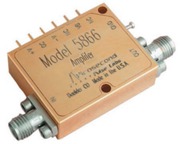
PSPL5866 10 GHz Linear Amplifier Datasheet
PSPL5866 Datasheet
Tektronix больше не продаёт продукты из этого технического описания.
Посмотреть бывшее в употреблении оборудование для тестирования Tektronix Encore.
Просмотреть информацию о технической поддержке и гарантии для этих продуктов.
Дополнительные сведения
- Amplifiers and Drivers
- Explore more Программное обеспечение models
Читать на веб-сайте:
PSPL5866 Datasheet
The PSPL5866 amplifier has been designed to minimize the variations in gain and phase and to operate at very low frequencies. The PSPL5866 includes internal temperature compensation for excellent output stability over temperature, and exhibits both high output and low power dissipation. It also incorporates internal sequencing circuitry, making it insensitive to power supply application sequence.
Key performance specifications
- Linear amplifier with 25 dB gain
- 2.5 kHz to 10 GHz bandwidth
- > 4 V p-p linear output
Typical performance
Typical S21 (measured at –22 dBM input power)

Typical S11 and S22 (measured at –22 dBM input power)

Typical linearity (measured with 400 mHz CW)

Typical response to 15 ps Rise time step

Input from Tektronix PPG1601, PRBS = 223–1, 200 mV

Output amplitude, 4 V
Instructions
The PSPL5866 amplifier may be operated using only three of the available 7 pins. The DC pins required for operation are 1, 3, and 7. The RF connectors and DC pins are diagramed and defined below.

| Pin # | Pin Lable | Description |
|---|---|---|
| IN | SMA, signal input, Vamp≤ 1.5 V (damage threshold) | |
| 1 | +V | Positive DC voltage supply, 8 V 12 |
| 2 | NC | No connection / Not used |
| 3 | -V | Negative DC voltage supply, -5.25 V ≤ V ≤ -4.75 2 |
| 4 | CP | Bias point adjust, -5 V ≤ Vcp≤ 1 V 3 |
| 5 | VB | DC Voltage bias, 0 ≤ VB ≤ +16 4 |
| 6 | NC | No connection / Not used |
| 7 | GND | Ground connection |
| OUT | SMA, signal output |
Warning: The PSPL5866 requires a ground connection at pin #7 prior to voltage application to prevent damage.
1 At +17 dBm output, approximately 1.7 W is dissipated.
2 No power sequencing is necessary. Voltages may be applied in any order after ground is applied.
3 The bias point may vary until unit achieves thermal equilibrium.
4 Voltage Bias: The VB pin allows the user to apply a low current (less than 3.5 mA) DC offset through an internal 2.5 kΩ resistor to the Signal Output.
Specifications
| Parameter | Symbol | Units | Minimum | Typical | Maximum | Comments |
|---|---|---|---|---|---|---|
| Impedance | Z | Ohms | 50 | |||
| Upper 3 dB freq. | fc,h | GHz | 8 | 10 | Relative to gain at 1 GHz | |
| Lower 3 dB freq. | fc,l | kHz | 2.5 | 3 | Relative to gain at 1 GHz | |
| Small Signal Gain | S21 | dB | 25.0 | 25.5 | Measured at 1 GHz | |
| Return Loss, Input and Output | S11, S22 | dB | -12 | -8 | 50 MHz | |
| Rise / Fall Time | tr,f | ps | 35 | 10-90% | ||
| Additive Jitter RMS Peak-to-peak |
ps pspp |
0.7 4 |
1.5 8 |
|||
| Eff. Input RMS Noise Voltage | NF | μV rms | 114 | |||
| Noise Figure | dB | 5.75 | 6.5 | f = 1 GHz | ||
| Max Power Out (-1 dB gain comp) |
dBm | 17 | Measured at 1 GHz | |||
| Polarity | Non-Inverting | |||||
| Coupling | AC, input and output | |||||
| RF Connectors | SMA jacks (f) | |||||
| DC Connector | Solder pin | |||||
| Supply Voltage (+) | +VDC | VDC | 8 | 8 | 8.25 | |
| Supply Voltage (-) | -VDC | VDC | -5.25 | -5 | -4.75 | |
| Supply Current (+) | +IDC | mA | 200 | 220 | Damage threshold | |
| Supply Current (-) | -IDC | mA | 20 | |||
| Power Dissipation | Pdiss | W | 1.7 | 2.0 | Vout = 4 Vp-p | |
| Max Allowed Input | Vamp | 1.5 | Input damage threshold | |||
| Bias Point Adjust | VCP | VDC | -5 | 1 | No connection required | |
| Output Voltage Bias | Vbias | VDC | 0 | 16 | No connection required | |
| Operating Temp | TCASE | Deg C | -5 | 75 | Case temperature | |
| Storage Temp | Tstor | Deg C | -40 | 125 | ||
| Warranty | One Year | |||||
Note: The PSPL5866 should be driven with a negative polarity signal when the duty cycle is very low. The amplifier may be damaged by excessive heat that is produced with narrow positive pulses. Similarly, signals with a very high duty cycle should be positive. To ensure the amplifier will not be damaged by overheating under such operating conditions, the positive supply voltage should have its current limit set to 220 mA.
The PSPL5866 is AC-coupled at the input and output. As a result, the average value of the output signal (the DC component) must be at 0 volts. Most data streams are conditioned to have 50% duty cycle when averaged over many microseconds. Those signals make full use of the positive and negative portions of the amplifier’s operating range.
The average amplitude of a low duty cycle signal can be virtually at the baseline. These signals use only one half of the PSPL5866’s operating range, and the maximum linear output may be 2 volts peak-peak instead of 4 volts peak-peak. Offsetting VCP will shift the amplifier’s operating range so that the amplifier’s 4-volt linear range is not centered on 0 V. The following graph shows these shifted operating ranges.

Input vs. Output for Model PSPL5866 using a 3 ns pulse with pulse repetition frequency of 100 kHz and Vcp = 0 V. The duty cycle is 0.03%. The PSPL5866 remains linear for inputs from -2 V to +2 V. The purple line shows 25.5 dB linear gain for comparison.

Input vs. Output as VCP is varied (–5 V
Mechanical dimensions

Ordering information
Models
- PSPL5866
- AMPLIFIER, 25 dB GAIN, 2.5 kHz-10 GHz