Kontaktaufnahme
Live-Chat mit Tektronix-Vertretern. Verfügbar von 9 bis 17 Uhr CET Geschäftstage.
Kontaktieren Sie uns telefonisch unter
Verfügbar von 9 bis 17 Uhr CET Geschäftstage.
Download
Laden Sie Handbücher, Datenblätter, Software und vieles mehr herunter:
Feedback

Einfach kompetent erledigt
Tektronix dient als Erweiterung Ihres Teams und bietet maßgeschneiderte Lösungen für Kalibrierdienste, die Zeit und Kosten sparen und die Genauigkeit von elektronischen Test- und Messgeräten gewährleisten. Wir arbeiten mit Ihnen zusammen, um die intelligentesten Geschäftsentscheidungen bei der Erweiterung oder Auslagerung von Kalibrierungen anspruchsvoller Prüf- und Messgeräte zu treffen. Täglich verlassen sich Tausende von Unternehmen bei der Bereitstellung von OEM-Qualitätskalibrierungen zu einem wettbewerbsfähigen Marktpreis auf Tektronix.
- Wartung von Tektronix, Keithley, Fluke, Keysight, Rohde & Schwarz, Agilent und mehr als 9.000 weiteren Prüf- und Messgerätemarken
- Maßgeschneiderte Programmoptionen: Vor-Ort-Service, Abholung, Lieferung bis Werk
- Schnelle, zuverlässige Bearbeitungszeiten
- Vollständige Palette nach Z540 und ISO 17025 akkreditierter Kalibrierungen
- A2LA-zertifizierte technische Fachkräfte
Understanding 2.5D Packaging vs. 3D Packaging
As semiconductor manufacturers start to reach the potential physical limits of shrinking process nodes, chip packaging is emerging as a way to improve performance. Flip chip assembly remains the most popular method for interconnecting dies, but new advancements in silicon interposers enabling 2.5D packaging architectures, and in-turn, making 3D packaging possible.
What is 3D Packaging?
Certainly. 3D packaging involves stacking multiple semiconductor dies (or chiplets) vertically, creating a three-dimensional packaging architecture. This approach enables closer integration of different components within a single package.
It is also worth noting that 3D Heterogeneous Integration (3DHI) is a sub-category of 3D packaging. The "heterogeneous" aspect implies that these dies may serve diverse functions and could come from various fabrications processes or vendors.
How is 2.5D and 3D Packaging different?
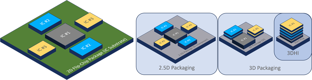
The key difference lies in the vertical stacking and bonding of components. Traditional packaging methods involve placing chips side by side on a flat surface, limiting the amount of integration that can be achieved. In 3D packaging, components are stacked on top of each other, reducing the distances between them and offering higher integration density.
What are the benefits of 2.5D & 3D Packaging?
There are many benefits to the 3D packaging approach, so for the sake of this conversation let’s just focus on Size, Weight, and Power (SWaP).
- Size Reduction: One of the most pronounced benefits of 3D packaging is its superior size efficiency. By vertically stacking semiconductor components within a single package, it dramatically reduces the physical footprint of package. This reduction in size is particularly valuable in applications where space is at a premium, such as mobile devices, aerospace systems, and wearable technology. As electronic devices continue to shrink in size, 3D packaging enables the creation of smaller, more compact products without compromising on performance.

- Weight Reduction: 3D packaging contributes to weight reduction in electronic systems. The compact and densely integrated design achieved through vertical stacking leads to a decrease in the overall weight of devices. This is of paramount importance in sectors like aerospace, where every gram counts. Lighter electronics can translate to more fuel-efficient aircraft and extended mission capabilities for unmanned aerial vehicles..
- Power Efficiency: In terms of power efficiency, 3D packaging has a twofold impact. Firstly, the vertical stacking of components often results in shorter interconnection lengths. Reduced distances for data to travel lead to lower signal losses and reduced power consumption. Secondly, the reduction in off-chip communication further enhances power efficiency. With components closely integrated within the 3D package, there's less need for energy-intensive data transmission between chips, resulting in overall energy savings.
As a proven US-based, ITAR-registered supplier to a variety of defense programs and companies, Tektronix Component Solutions is an ideal partner for defense applications requiring high-performance, mission-critical microelectronics. Offering services and products that include wafer test, IC packaging assembly and test, 2.5/3D packaging, and design & simulation, Tektronix Component Solutions has the expertise and capabilities to meet your requirements for high-reliability microelectronics.
With more than 40 years of experience, Tektronix Component Solutions is the stable supplier that you can trust to deliver on long-term military programs.
Trusted, ITAR-Registered Supplier
Tektronix Component Solutions has been accredited by the U.S. Department of Defense (DOD), Defense Microelectronics Agency (DMEA) as a Category 1A microelectronics Trusted Source for IC packaging/assembly and test services – the highest designation awarded by the U.S. Department of Defense. This enables Tektronix Component Solutions to serve U.S. defense customers with classified program requirements. The accreditation certifies that Tektronix Component Solutions meets stringent product control and security standards in providing trusted microelectronic services. Tektronix Component Solutions also holds certifications in ISO9001/ISO14001 and AS9100D and meets all ITAR requirements.
As an on-shore, ITAR-registered supplier, Tektronix Component Solutions has stringent standards in-place to protect and control sensitive information related to defense programs. With many years of experience supporting defense customers and programs, we recognize and adhere to the added level of responsibility in providing microelectronic engineering and manufacturing services to the military.
High-Performance Products and Services
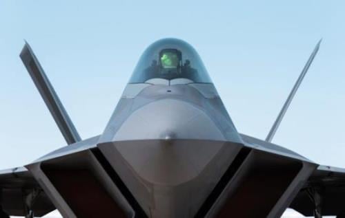
Our military experience spans a variety of critical applications, including communications, avionics, radar, propulsion control, and guidance systems. Tektronix Component Solutions has supplied high-performance and high-reliability products to defense programs such as the F-22 Raptor and F-35 Lightning II (Joint Strike Fighter) with a focus on continual C-SWaP (cost, size, weight and power) improvements.
Having served military and commercial aerospace customers for many years, Tektronix Component Solutions has a deep understanding of the high-reliability requirements of those applications. As such, we fully utilize our unique strength in test to deliver fully-tested parts that have proven to operate successfully in mission-critical environments.
Request More Information
Frequently Asked Questions (FAQ)
What is a high-level overview of the process for packaging?
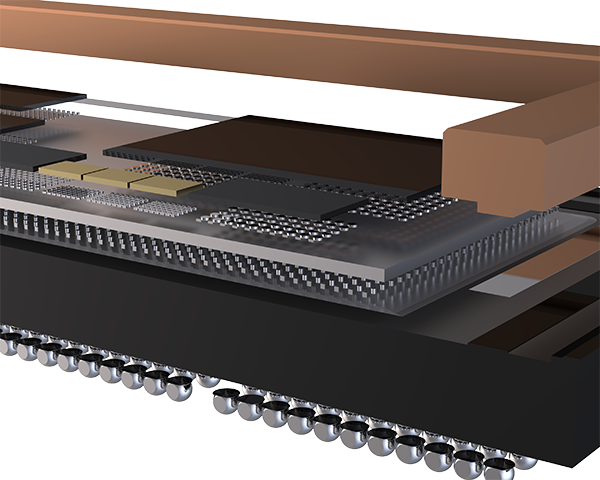
Once upon a time, packaging was primarily done with wire bonding and surface-mount technology. Today, flip chip is still the gold standard. The progression of flip-chip, integrated circuit (IC) packaging is important. In its most basic form, IC packaging facilitates fanout of the semiconductor device interconnects to meet the technology restrictions of the board that it will be placed on. Manufacturing constraints of the system level board prevent IC’s from being mounted directly for a variety of reasons, such as interconnect density limitations, product reliability concerns, and rework restrictions.
Single or multiple chips are therefore placed on the package substrate. This minimizes electrical performance loss, maintaining signal and power integrity, while also improving overall reliability. Reliability is also enhanced by pairing the silicon chips with specifically designed materials to address coefficient of thermal expansion (CTE) because mismatch stresses can lead to early system-level failure.

Since the advent of flip-chip technology, packages have evolved to reduce cost, size, weight and power (CSWaP). Overall, a smaller footprint—we can do more in less space with less power at a lower cost. This is of particular interest in military and aerospace deployments, which required stringent reliability standards.
As silicon interconnect densities have increased, so too have the interconnect densities of high-density-build-up (HDBU) style package substrates. At least to a point. It’s anticipated that minimum interconnect densities will bottom out around 125um pitch, perhaps ranging slightly lower. This presents an issue in the context of CSWaP, since die interconnect densities of 5um pitch are possible today.
What has changed in product architecture today to address this?
Historically, when you see advancements in semiconductor performance, it was frequently done through the miniaturization of die through front end manufacturing improvements and shrinking process nodes. But semiconductors are starting to reach the limit of improvements in front end manufacturing. Cost is the primary limitation today, but the physics of fitting more transistors in the space available is starting to show diminishing returns.

Beginning with single-chip package architecture, increased semiconductor die sizes were the first evolution with monolithic silicon chips. The aim was do more on one chip in less space. However, larger silicon and more delicate active layers led to reduced product reliability. It also led to increased difficulty characterizing the product using existing packaging methods. Silicon turns are also very costly, making this progression unappealing for die sizes approaching 20mm.
The second architecture iteration was the beginning of what the industry is calling “disaggregation” or splitting out of various functions into multiple die. The concept of multi-chip modules is not new but is being revisited in support of CSWaP objectives. This package style is common in industry today and facilitates more effective product optimization during development and flexibility down the line. We have several multi-chip module (MCM) style products from external customers in active production today.
The third iteration, titled 2.5D heterogeneous integration, leverages semiconductor technology and disaggregation to do more in less space by adding another interposer—silicon, glass, silicon carbide—between the substrate and high density silicon devices or “chiplets.” 2.5D is becoming very important in the industry, and is something that I could talk about in-length, but maybe that’s better saved for its own interview.
What challenges arise when working at such a small scale?
Process assembly methodology, while more challenging compared to legacy package designs, is largely understood today. New challenges exist with product design methods, like software tools and design flow. There are also challenges with thermal solutions, needing to address increasing power densities, and electrical test capability. As products become more advanced and disaggregated from a functionality point of view, the concept of “known-good-die” is much more difficult to quantify. Chip-to-chip interactions can influence end performance in unpredictable ways, making wafer test a necessity but also a challenging cost tradeoff. End item product testing is an absolute necessity, but development work is also needed to ensure testing at various stages of assembly are deployed judiciously to ensure proper end item yield. Design for test is also an increasing area of focus for these architectures.
What opportunities are there for performance improvement today?
The more we miniaturize packaging and not just the process node, the better the performance we’ll see from the assembled device. The use of interposers is the next evolution in this arena. Shorter electrical connections provide higher bandwidth and lower loss solutions. Disaggregation, or the use of “chiplets” as it’s called, can facilitate better product characterization and customization. 2.5D architectures can significantly bolster CSWaP initiatives. So, as I mentioned, 2.5D packaging is a big focus in the industry today, and a significant priority for our team at Tektronix.
What are the challenges that gate 3D packaging adoption?
Indeed, the adoption of 3D packaging is in its early stages, and it's important to address several critical challenges before widespread implementation can occur. Let's delve into some of these challenges, particularly focusing on design considerations for manufacturing (DFM), design for test (DFT), and design for reliability (DFR):
- Design for Manufacturing (DFM): As 3D packaging technologies mature, ensuring efficient and cost-effective manufacturing processes becomes paramount. DFM principles need to be integrated into the design phase to minimize manufacturing complexities and costs. Designers must consider factors like material choices, process compatibility, and yield optimization.
- Design for Test (DFT): Thorough testing of 3D-integrated systems poses unique challenges due to their vertically stacked nature. Designing for testability is critical to develop test strategies that can comprehensively evaluate the functionality and reliability of all components within the 3D package. DFT methodologies need to address accessibility and coverage concerns in the stacked configuration.
- Design for Reliability (DFR): 3D packaging introduces new reliability considerations, particularly concerning thermal management, stress, and interconnect reliability. Designers must incorporate DFR principles to ensure that the vertically stacked components can withstand environmental stresses, maintain signal integrity, and have a long operational lifespan.
In conclusion, 3D packaging adoption faces significant challenges as these technologies are deployed in harsh environments, factors like design for manufacturing, design for test, and design for reliability will be critical to ensure the success and longevity of 3D-integrated systems. As the industry addresses these challenges, we can expect to see greater adoption of 3D packaging in various applications.