

Test and Measurement Equipment


Contact us
Call
Call us at
Available 6:00 AM – 5:00 PM (PST) Business Days
Download
Download Manuals, Datasheets, Software and more:
Feedback


Solutions and Applications


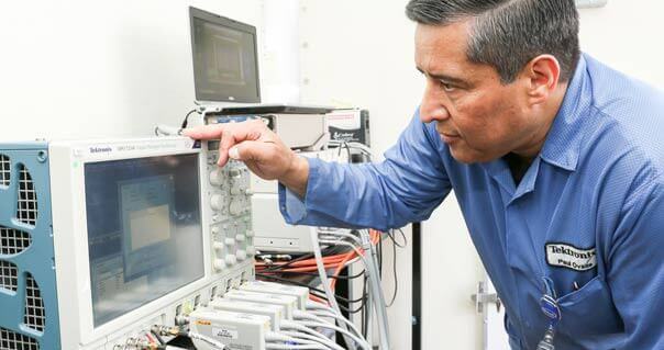
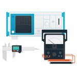
Calibration & Services
We calibrate more than 140,000 products from 9,000 different manufacturers, far more than just Tektronix and Keithley equipment. Tektronix offers manufacturer quality calibration for all of your electronic test and measurement equipment.
Learn More About CalibrationSee All Services


