Current Language
×
Chinese (Traditional, Taiwan)

選取語言:

切換功能表
Current Language
×
Chinese (Traditional, Taiwan)

選取語言:

與我們聯絡

與 Tek 業務代表即時對談。 上班時間:上午 6:00 - 下午 4:30 (太平洋時間)

致電

請致電

與 Tek 業務代表即時對談。 上班時間:上午 8:30 - 下午 5:30 (太平洋時間)

下載

下載手冊、產品規格表、軟體等等:

下載類型
機型或關鍵字

意見回饋

Measuring MOSFET Gate Charge with the 4200A-SCS Parameter Analyzer


Introduction

Power MOSFETs are used in a variety of applications and can be used as high-speed switching. The switching speed of the device is affected by internal capacitances, which is typically specified in data sheets in terms of Ciss and Coss, which are derived from the input gate and drain capacitance, Cgs and Cgd. In addition to specifying the capacitance, the gate charge (Qgs and Qgd) can also be used to assess the switching performance of the MOSFET.

One method of measuring the gate charge of a MOSFET gate charge is described in the JEDEC JESD24-2 standard, "Gate Charge Test Method". In this method, a gate current is forced while the gate to source voltage is measured as a function of time. From the resulting gate voltage waveform, the gate-source charge (Qgs), gate-drain charge (Qgd), and gate charge (Qg) are derived.

The 4200A-SCS Parameter Analyzer supports making MOSFET gate charge measurements using two source measure unit (SMU) instruments and the gate charge measurement test that's included on the system. This test is one of many included in the extensive Test Library provided in the 4200A-SCS Clarius+ Software Suite. This application note describes how to measure MOSFET gate charge based on the JEDEC Gate Charge Test Method using the 4200A-SCS Parameter Analyzer.

MOSFET Gate Charge Measurement Overview

In the Gate Charge Method, a fixed test current (Ig) is forced into the gate of a MOS, transistor and the measured gate source voltage (Vgs) is plotted against the charge flowing into the gate. A fixed voltage bias is applied to the drain terminal. Figure 1 shows the gate voltage vs. gate charge of a power MOSFET.

The gate charge (Q) is derived from the forced gate current and time, (Igdt). The gate-source charge (Qgs) is the charge required, as shown in Figure 1, to reach the beginning of the plateau region where the voltage (Vgs) is almost constant. The plateau (or Miller) voltage (Vpl) is defined, according to the JEDEC standard, as the gate-source voltage when dVgs/dt is at a minimum. The voltage plateau is the region when the transistor is switching from the OFF state to the ON state. The gate charge required to complete this switching—the charge needed to switch the device from the beginning of the plateau region to the end—is defined as gate-drain charge (Qgd) and is known as the Miller charge. The gate charge (Qg) is the charge from the origin to the point where the gatesource voltage (Vgs) is equal to a specified maximum (VgsMax).

 
MOSFET gate charge measurement graph showing voltage vs. gate charge of a power MOSFET
Figure 1. Typical gate voltage vs. gate charge of power MOSFET
 

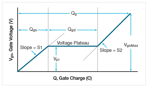
S1 is the slope of the line segment from the origin to the first plateau point. S2 is the slope of the line segment from the last plateau point to the specified maximum gate voltage (VgsMax). The slopes are used to calculate Qgs and Qgd, as specified in the JESD24-2 standard.

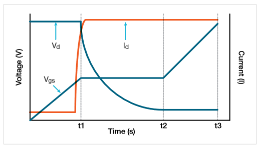
Figure 2 shows typical gate and drain waveforms as a function of time. As current is forced to the gate, Vgs increases until it reaches the threshold voltage. At this point, the drain current (Id) begins to flow. When Cgs is charged up at time t1, Id stays constant and the drain voltage (Vd) decreases. Vgs remains constant until it reaches the end of the plateau. Once Cgd is charged at time t2, the gate-source voltage (Vgs) starts to increase again until it reaches the specified maximum gate voltage (VgsMax).

 
Graph showing gate and drain waveforms as a function of time
Figure 2. Vgs, Vd, and Id vs. time of MOSFET
 

Using the 4200A-SCS for MOSFET Gate Charge Measurements

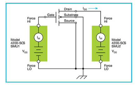
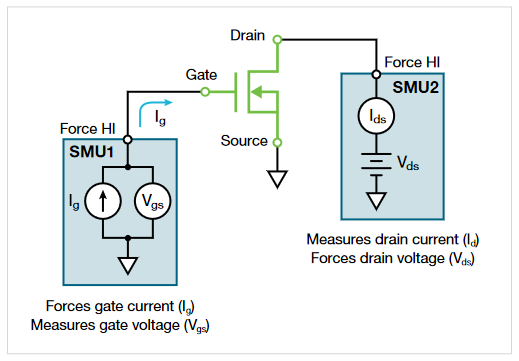
The 4200A-SCS measures gate charge of a power MOSFET using two SMU instruments. Figure 3 illustrates the basic circuit diagram of the gate charge test. The Force HI terminal of one SMU (SMU1) is connected to the gate terminal of the MOSFET and forces the gate current (Ig) and measures the gate-source voltage (Vgs) as a function of time. A second SMU (SMU2) applies a fixed voltage (Vds) to the drain at a specified current compliance (Ib). The maximum compliance current of the 4200-SMU is 0.1 A; the maximum compliance of the 4210-SMU is 1 A.

During the gate charge test, the gate voltage increases and turns ON the transistor. During this transition in the plateau region, the drain SMU (SMU2) switches from voltage control to the current control mode, because the current exceeds the specified compliance level. The software returns the drain current transients and drain voltage during the transition from the OFF state to the ON state.

The MOSFET's source terminal is connected to the Force LO terminal or GNDU of the 4200A-SCS chassis.

 
MOSFET gate charge test configuration using two source measure unit (SMU) instruments
Figure 3. Gate charge test configuration using two SMU instruments.
 

Configuring the Clarius+ Software for MOSFET Gate Charge Measurements

The Gate Charge test is located in both the Test and Project Libraries, which can be found in the Select pane by searching for the phrase "gate charge". Once the test is found in the Test Library, it can be added to a project by selecting and adding it to the project tree. This test was created from the gate_charge user module in the GateCharge user library.

Enter Input Parameters

Before test execution, you need to enter the input test parameters in the Configure pane of the Clarius Software (Figure 4). The input parameters will vary depending on the device and which model of SMU is used.

 
Setting up a MOSFET gate charge test in the configuration view of the Keithley Clarius software
Figure 4. The gate charge test in the Configure View.
 

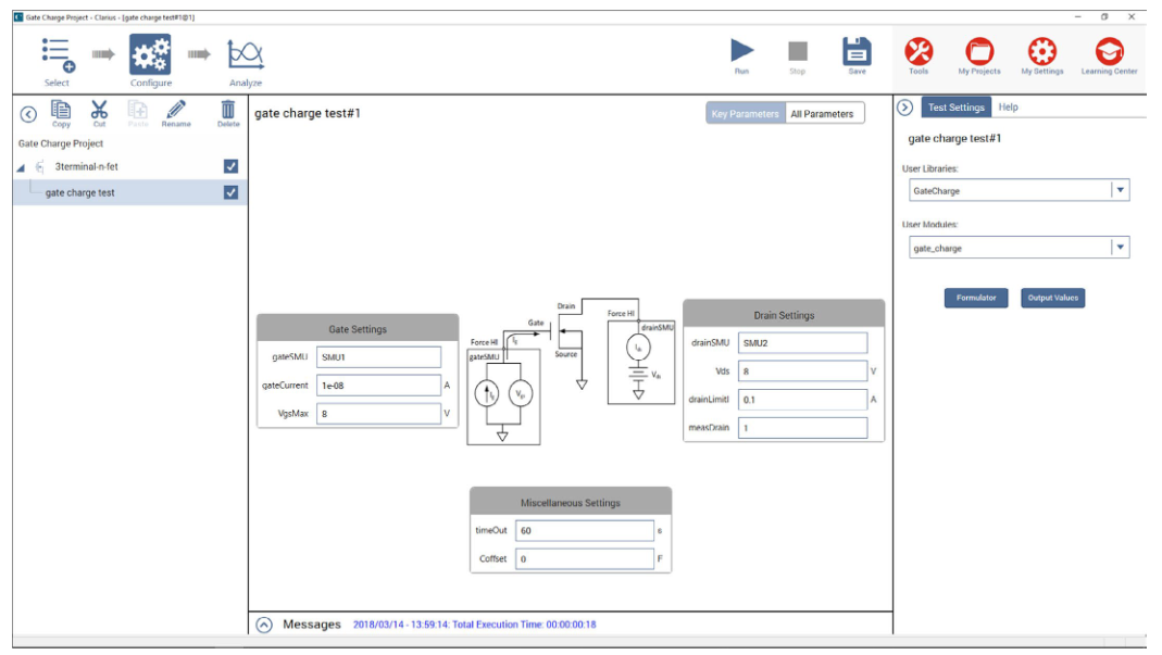
Descriptions of the input parameters are listed in Table 1. First, enter the SMU numbers that are connected to the gate (gateSMU) and drain (drainSMU) of the MOSFET. The source terminal should always be connected to the GNDU, or Force LO.

The magnitude of the current forced to the gate by the gateSMU, is the gateCurrent (Ig) parameter. The drain voltage (Vds) is the bias voltage applied to the drain and drainLimitI is the compliance current of the drain SMU.

The Coffset parameter is used for correcting for the offset capacitance and is described in the following paragraphs.

Table 1. Input Parameters for gate_charge user module.

Input Parameter Range of Values Default Values Description
gateSMU SMU1-SMU9 SMU1 The SMU number connected to the gate terminal
drainSMU SMU1-SMU9 SMU2 The SMU number connected to the drain terminal
source GNDU GNDU The source terminal is always connected to the Force LO terminal on GNDU
Vds ± 200 V 10 V The magnitude of the drain bias voltage of the drain SMU
drainLimitI 4200-SMU: 0.1A
4210-SMU: 1 A
0.1 A Current compliance of the drain SMU
gateCurrent ± 1E-5 A 1e-7 A The magnitude of the gate current of the gate SMU
VgsMax ± 200V 10 V The maximum voltage level of the gate SMU.
timeOut 0 to 300 s 60 s The number of seconds prior to a time out.
measDrain 1 (yes) or 0 (no) 1 Return measured drain current
Coffset 0 or Ceff 0 Run test with open circuit and then enter Ceff value returned to the Sheet


Correct for Offset Capacitances

Depending on the cabling and connections of the measurement system, the offset capacitance can be in the single picofarads to hundreds of picofarads ranges. These capacitances can be corrected by executing the gate_charge user module with an open circuit, obtaining the offset capacitance, then entering the offset capacitance value in the software for compensation. Here's how to perform these steps:

  1. Measure the offset capacitance. Set up the test parameters including the input gate current as though the device were connected to the SMUs. (Increase the VgsMax just for the Ceff measurement.) Prior to executing the test, lift the probes or remove the device from the test fixture. Execute the Gate Charge test with an open circuit.
  2. Obtain the offset capacitance. After the test is executed, the measured offset capacitance of the system is calculated and appears in the Ceff column in the Sheet. Ceff is derived from the maximum gate voltage, gate current, and time.
    Because an open circuit is measured during this step, a Test Status Value of -9 or -12 may appear in the Sheet after the test is executed. This is because no device is measured so there is no plateau region. However, the Ceff value is correct and can be entered as the Coffset in the Configure view.
  3. Enter the measured offset capacitance and execute. Enter the measured offset capacitance, Ceff, for Coffset in the Configure view. By default, Coffset is 0 F. Compensation will be made for the offset capacitance in subsequent readings.

Execute the Test

Once the input parameters have been entered, execute the test by selecting Run at the top of the screen. As the test is running, the gate charge waveform will update in real time in the graph in the Analyze view and the calculated output parameters will appear in the Sheet.

View Output Parameters

After the test is completed, several parameters are returned to the Sheet. Table 2 lists descriptions of these parameters.

Table 2. Output parameters for gate_charge user module

 
Output Parameter Description
gate_charge Test status values - see Table 3 for descriptions
timeArray Measured time (seconds)
VgArray Measured gate-source voltage (volts)
VgCharge Measured gate charge (coulombs)
VdArray Measured drain voltage (volts)
IdArray Measured drain current (amps)
Slope Dynamic slope (dVg/dt) of gate voltage
Ceff Ratio of gate charge to maximum gate voltage
Vpl Plateau or Miller voltage (volts)
T1 Timestamp where the plateau area begins (seconds)
T2 Timestamp where the plateau area ends (seconds)
Qgs Gate charge from the origin to the first inflection point, or the voltage plateau (coulombs)
Qgd Gate charge between the two inflection points in the gate charge curve (coulombs)
Qg Gate charge from the origin to VgsMax (coulombs)


Graphing the Results

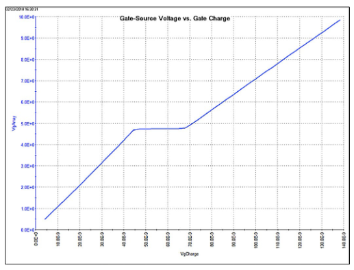
The resulting gate-source voltage can be plotted as a function of the gate charge or the drain current, and drain voltage can be plotted as a function of time. Figure 5 is a typical gate voltage waveform generated by the 4200A-SCS

 
MOSFET gate voltage waveform generated by the Keithley 4200A-SCS parameter analyzer
Figure 5. Typical gate voltage waveform generated by the 4200A-SCS.
 

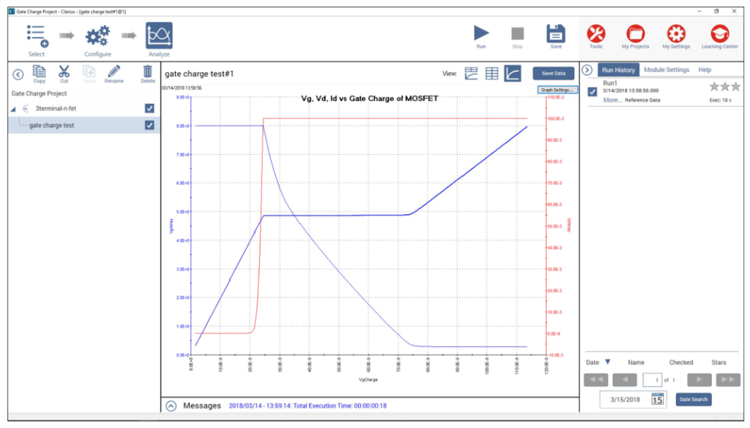
In addition to plotting Vgs, Vds, and Id can also be plotted as a function of the MOSFET gate charge or time. Figure 6 shows the graph in the Analyze view of the Clarius Software showing all three parameters plotted as a function of the gate charge. In this case, the voltage is shown on the Y1 axis and the current is plotted on the Y2 axis.

 
Vgs, Vds, and Id as a function of MOSFET gate charge over time
Figure 6. Vgs, Vds, and Id as a function of gate charge.
 

Check the Test Status

Each time the test is executed, a Test Status Value is returned to the first column in the Sheet, named "gate_charge". Table 3 lists the returned Test Status Values in the "gate_charge" column and their corresponding descriptions and notes.

Table 3. Test Status Values

Test Status Description Notes
1 No errors Test successful.
-1 Gate SMU is not present Specify correct SMU.
-2 Drain SMU is not present Specify correct SMU.
-3 VgsMax > 200 V Verifies gate voltage is less than 200V. Reduce gate voltage.
-4 Drain current limit exceeds 1 A (4210-SMU)
Drain current limits exceeds 0.1 A (4200-SMU)
Verifies drain current is less than 1 A (or 0.1A for medium power SMU). Reduce drain current limit (drainLimitI).
-5 Power limit exceeded Current should be < 0.1A if V >20V. Decrease drain current limit (drainLimitI) or drain voltage (Vds).
-6 Error check on input conditions. Limits timeOut to 200 s. Specify timeOut to <200 s.
-7 Test time exceeds specified time out (timeOut). Increase timeOut. Maximum is 200 s. Try increasing gateCurrent to charge up device faster.
-8 Number of iterations/measurements >10000. Increase gate current (gateCurrent).
-9 Number of iterations/measurements <5 Decrease gate current (gateCurrent). Check device, test set-up and for correct SMU.
This error can be ignored if it occurs while measuring an open circuit for offset correction. The Ceff value is still valid.
-10 Number of points from origin to first plateau point is <10 Decrease gate current (gateCurrent)
-11 Error calculating slope, S1. Correlation factor < 0.9. Curve from origin to first plateau point is not linear. Check device and test set-up.
-12 Error calculating slope, S2. Correlation factor <0.9. Curve from last plateau point to VgsMax is not linear. Check device and test set-up. If VgCharge or VdArray appear high,try reducing gateCurrent and repeat test.
This error can be ignored if it occurs while measuring an open circuit for offset correction. The Ceff value is still valid.
-13 Vds > 200 V Decrease drain voltage.
-14 gateCurrent > 10 µA Decrease gate current (Ig).


Conclusion

MOSFET gate charge measurements on transistors can be easily made using the Keithley 4200A-SCS Parameter Analyzer. Using two SMU instruments connected to the gate and drain of the device, the Clarius Software easily derives the gate charge waveforms.

Find more valuable resources at TEK.COM

資源

fig-18
小冊子

建立類似於雷達的訊號

哪種最佳解決方案可協助您在最高頻率建立複雜的雷達測試訊號?我們的應用說明涵蓋了建立可以瞞過您雷達系統的訊號之最佳方法。

smu
部落格

進階雷達分析:現代雷達量測的工具

降低設計過程中的測試不確定性,並為日益複雜的設計建立信心。此應用摘要會一一解析,針對現代化的雷達時,您不可或缺的工具。

SMU Group
部落格

電子對抗的驗證技術

本次網路研討會探討了使用 Tektronix 即時頻譜分析儀 (例如 RSA5100B 和 RSA7100B),來驗證電子對抗 (ECM) 系統的方法。

Noisey gate drive
部落格

電子對抗的驗證技術

本次網路研討會探討了使用 Tektronix 即時頻譜分析儀 (例如 RSA5100B 和 RSA7100B),來驗證電子對抗 (ECM) 系統的方法。

Mosfet Gate Charge Frequently Asked Questions

What is the drain-source on-resistance of a MOSFET?

MOSFET switching devices operate in the on and off states. In the “on” state, the impedance of the switch is theoretically zero and no power is dissipated in the switch no matter how much current is flowing through it. In the “off” state, the impedance of the switch is theoretically infinite, therefore no current is flowing and no power is dissipated.

Thedrain-source on-resistance (RDS(on)) is the effective resistance between the drain and the source of a MOSFET when it’s in the on state. This occurs when a specific gate-to-source voltage (VGS) is applied. In general, as the VGS increases, the on-resistance decreases. The lower the MOSFET on-resistance, the better because a low resistance reduces undesired power dissipation, improving the power efficiency of the device.

How can I test a MOSFET for drain-source on-resistance on my curve tracer?

Answer: Drain-Source On-Resistance - RDS(on)

What is drain-source on-resistance?

Drain-source on-resistance (RDS(on)) is the resistance between the drain and the source of a MOSFET when a specific gate-to-source voltage (VGS) is applied to bias the device to the on state. As the VGS increases, the on-resistance generally decreases. The measurement is made in the ohmic (i.e. linear) region of the device. Generally speaking, the lower the MOSFET on-resistance, the better.

One of the ways to trace this resistance is to use a curve tracer. On a curve tracer, the so called “Collector Supply” drives the drain while the “Step Generator” drives the gate. For step-by-step instructions on how to test a MOSFET for drain-source on-resistance using a curve tracer, see below. For instructions on how to use an oscilloscope or SMU to measure MOSFET on-resistance, see our “What is the drain-source on-resistance of a MOSFET?” FAQ.

What the display shows:

The display shows VDS on the horizontal axis, and the resulting ID on the vertical axis. The specification is met when at the specified VDS, VDS/ID is less than or equal to the specified maximum.

How to test a MOSFET for drain-source on-resistance on a curve tracer:

1. Under Controls, set:

            A:Max Peak Volts to the lowest setting above the specified VDS

            B: Max Peak Power Watts to the lowest setting that satisfies (ID x VDS)

            C: Collector Supply Polarity to (+DC) for N-channel or (-DC) for P-channel  

            D: Horizontal Volts/Div to display VDS between the 5th and 10th horizontal divisions

            E: Vertical Current/Div to display ID between the 5th and 10th vertical divisions

            F: Number of steps to minimum (zero)

            G: Step Generator to Voltage

            H: Step Generator Polarity to apply forward bias (+ for N-channel), (- for P-channel)

            I: Step/Offset Ampl to approx 50% of the specified VGS

            J: Pulse to Long       

            K: Configuration to (Base/Step Gen, Emitter/Common)

            L: Variable Collector Supply to minimum % (full ccw)

            M: DotCursor ON

2. Apply power to the MOSFET:

            A: Position the Left/Right switch as appropriate

            B: Slowly increase the Variable Collector Supply until the specified VDS is reached

3. Compare to data sheet specifications:

            A: Check that VDS/ID is less than or equal to the specified minimum

Tektronix Curve Tracers are discontinued products. More efficient and accurate methodologies and solutions have been designed to support curve tracing functionality on a much more compact form factor. One such solution is based on using a dual channel SMU or two single channel SMUs and software to control the bias voltage step generation and the relative drain to source voltage drop. To learn more, see our “What is the drain-source on-resistance of a MOSFET?” FAQ.

How do you find the transconductance of a MOSFET?

Transconductance is a key test for validating the MOSFET performance in power electronics designs. It ensures that a MOSFET is functioning properly and helps engineers choose the best one when voltage gain is a key spec for their circuit designs. This, in turn allows companies to take power semiconductor devices to market faster while minimizing failures in the field.

Transconductance is the ratio of drain current (ID) to gate-source voltage (VGS) when a constant drain-source voltage is applied. The current to voltage ratio is commonly referred to as gain. Transconductance is a critical parameter strictly connected with the threshold voltage (VTH) of MOSETs and both are related to the size of the gate channel. The formula for deriving the transconductance of a MOSFET from I-V measurements is:

gm = ΔID / ΔVGS

How to measure transconductance of a MOSFET?

The approach shown in the first configuration calls for three source measure units (SMUs), allowing every node to be held at a feedback-controlled voltage and every current to be measured simultaneously. If you don’t have enough SMU channels to cover each device channel connection, it is possible to proceed as shown in the second configuration. It should be noted that this configuration is more susceptible to a noisy ground connection and can produce ground loops if long cables are used. Also, the current and voltage at the source terminal cannot be measured, which can lead to errors in calculations.

Measuring transconductance

  1. Sweep the gate voltage (VGS) over the desired range, while maintaining a constant drain/source voltage (VDS)
  2. Measure the drain current (ID) at each increment step of VGS.
  3. Calculate transconductance (gm) by dividing the small changes in the current ID by the small changes in VGS.

The red plot line shown here illustrates the transconductance (gm) and the maximum transconductance value (Vth).

Learn more about safe, precise and fast MOSFET device characterization tests.

How can I test a MOSFET for Zero Gate Voltage Drain Current on my curve tracer?

Answer: Zero Gate Voltage Drain Current - IDSS

What is Zero Gate Voltage Drain Current? 

Zero gate voltage drain current is the ID that flows when VGS=0.  It’s the on-state current in a depletion mode MOSFET and the off-state current in an enhancement mode MOSFET.

On the IV curve tracer, the Collector Supply drives the drain and the gate is shorted to the source so that VGS=0.

What The Display Shows:

The display shows VDS on the horizontal axis, and the resulting ID on the vertical axis.  The specification is met when with VGS=0 and the specified VDS applied, ID is less than or equal to the specified maximum.

How To Do It:

1. Set controls:

            A:Max Peak Volts to the lowest setting above the specified VDS

            B: Max Peak Power Watts to the lowest setting that satisfies (ID x VDS)

            C: Horizontal Volts/Div to display VDS between the 5th and 10th horizontal divisions

            D: Vertical Current/Div to display the ID between the 5th and 10th vertical divisions

            E: Collector Supply Polarity to (+DC) for N-channel or (-DC) for P-channel

            F: Configuration to (Base/Short, Emitter/Common)

            G: Variable Collector Supply to minimum % (full ccw)

            H: DotCursor ON

2. Apply power to the MOSFET:

            A: Position the Left/Right switch as appropriate

            B: Slowly increase the Variable Collector Supply % until the specified VDS is reached

3. Compare to data sheet specifications:

            Check that at the specified VDS, ID is less than or equal to the specified maximum

How can I test a MOSFET for Gate Threshold Voltage on my curve tracer?

Answer: Gate Threshold Voltage - VGS(th)

What is Gate Threshold Voltage? 

Gate threshold voltage is the lowest VGS at which a specified small amount of ID flows.  The test is run with VGS = VDS.

On the curve tracer, the Collector Supply provides VDS.  Patch cords are used to short the gate to the drain so that VGS=VDS.

What The Display Shows:

VGS is displayed on the horizontal axis, and the resulting ID is displayed on the vertical axis.  The specification is met when, at the specified ID, VGS is within the min/max limits.

How To Do It:

1. Set controls:

            A: Max Peak Volts to the lowest setting above the specified VGS

            B: Max Peak Power Watts to the lowest setting that satisfies (ID x VDS)

            C: Horizontal Volts/Div to display VGS between the 5th and 10th horizontal divisions

            D: Vertical Current/Div to display the specified  ID between the 5th and 10th vertical divisions

            E: Collector Supply Polarity to (+DC) for N-channel or (-DC) for P-channel

            F: Configuration to (Base/Open, Emitter/Common)

            G: Variable Collector Supply to minimum % (full ccw)

            H: DotCursor ON

2: Attach patch cords:

            A: Connect a patch cord between the base and collector terminals on the unused side of the interface area

            B: Connect a second patch cord between the base sense and collector sense terminals on the unused side of the fixture area

3. Apply power to the MOSFET:

            A: Position the Left/Right switch to Both

            B: Slowly increase the Variable Collector Supply % until either the specified ID or the maximum threshold voltage is attained – whichever comes first

4. Compare to data sheet specifications:

            Check that the gate threshold voltage is within the specified min/max limits

How can I test a MOSFET for Transconductance (gFS) and Forward Admittance on my curve tracer?

Answer: Transconductance (gFS) and Forward Admittance

What is Transconductance and Forward Admittance? 

Transconductance is the ratio of ID to VGS.  The I/V ratio is commonly referred to as gain.

On the curve tracer, the Collector Supply drives the drain and the Step Generator drives the gate.

What The Display Shows:

The display shows VDS on the horizontal axis, and the resulting ID on the vertical axis.  With the Step Generator providing gate drive, the curve will be displaced upward from the horizontal axis as the gate drive causes a proportional ID.  The specification is met when, at either the specified VGS or the specified ID, the ratio of ID to VGS is equal to or greater than the specified minimum.

How To Do It:

1. Set controls:

            A:Max Peak Volts to the lowest setting above the specified VDS

            B: Peak Power Watts at the lowest setting to satisfy (ID x VDS)

            C: Collector Supply Polarity to (+DC) for N-channel or (-DC) for P-channel

            D: Horizontal Volts/Div to display the specified VDS between the 5th and 10th horizontal divisions

            E: Vertical Current/Div to display the specified ID between the 5th and 10th vertical divisions

            F: Number of steps to minimum (zero)

            G: Step Generator to Voltage

            H: Step Generator Polarity to apply forward bias  (+ for N-channel),  (- for P-channel)

            I: Step/Offset Ampl to approx 1% of the specified VDS

            J: Pulse to Long       

            K: Configuration to (Base/Step Gen, Emitter/Common)

            L: Variable Collector Supply to minimum % (full ccw)

            M: DotCursor ON

2. Apply power to the MOSFET:

            A: Position the Left/Right switch as appropriate

            B: Slowly increase the Variable Collector Supply % until the specified  VDS is reached

3. Adjust to parameters:

            Press and hold Offset Aid until an appreciable vertical displacement of the   curve occurs. It will be necessary to readjust Variable Collector % to maintain VDS.  Continue adjusting Step Offset and VDS alternately until the specified operating point is reached.

4. Calculate transconductance (gFS):

             Read gFS directly from the cursor readout

5. Compare to data sheet specifications:

              Check that the value is equal to or greater than the specified minimum

Forward admittance is an alternative way of expressing transconductance and is measured by setting the curve tracer up to measure transconductance (as above), switching Horizontal Volts/Div to STEP GEN, using SWEEP to complete the curve, then changing the cursor to F line and positioning the slope of the F line until it’s tangent to the curve.

How can I test a MOSFET for On-State Drain Current on my curve tracer?

Answer: On-State Drain Current - ID(on)

What is On-State Drain Current?

On-state drain current is ID with a specified VGS to bias the device to the on-state.  The measurement is made in the ohmic (i.e. linear) region of the device.

On the curve tracer the Collector Supply drives the drain and the Step Generator drives the gate.

What The Display Shows:

The display shows VDS on the horizontal axis, and the resulting ID on the vertical axis.  The specification is met when at the specified VDS, ID is greater than or equal to the specified minimum.

How To Do It:

1. Set controls:

            A:Max Peak Volts to the lowest setting above the specified VDS

            B: Max Peak Power Watts to the lowest setting that satisfies (ID x VDS)

            C: I: Collector Supply Polarity to (+DC) for N-channel or (-DC) for P-channel  

            D: Horizontal Volts/Div to display VDS between the 5th and 10th horizontal divisions

            E: Vertical Current/Div to display ID between the 5th and 10th vertical divisions

            F: Number of steps to minimum (zero)

            G: Step Generator to Voltage

            H: Step Generator Polarity to apply forward bias (+ for N-channel),  (- for P-channel)

            I: Step/Offset Ampl to approx 50% of the specified VGS

            J: Pulse to Long       

            K: Configuration to (Base/Step Gen, Emitter/Common)

            L: Variable Collector Supply to minimum % (full ccw)

            M: DotCursor ON

2. Apply power to the device:

            A: Position the Left/Right switch as appropriate

            B: Slowly increase the Variable Collector Supply until the specified VDS is reached

3. Compare to data sheet specifications:

            A: Check that ID is equal to or greater than the specified minimum

How can I test a MOSFET for drain-source breakdown voltage on my curve tracer?

Answer: Drain-Source Breakdown Voltage - V(br)DSS

What is Drain-Source Breakdown Voltage?

Drain-source breakdown voltage is the VDS at which a specified value of ID flows, with VGS=0.  Since it's the reverse current through a pinched-off channel, ID exhibits a knee shaped rise, increasing rapidly once breakdown occurs.

On the curve tracer, the Collector Supply drives the drain and the gate is shorted to the source so VGS=0.

What The Display Shows:

The display shows VDS on the horizontal axis, and the resulting ID on the vertical axis.  The specification is met when, at the specified ID, VDS is greater than or equal to the specified minimum.

How To Do It:

1. Set controls:

A: Max Peak Volts to the lowest setting above the specified minimum

     VDS

            B: Max Peak Power Watts to the lowest setting that satisfies (ID x VDS)

            C: Horizontal Volts/Div to display VDS between the 5th and 10th horizontal divisions

            D: Vertical Current/Div to display ID between the 5th and 10th vertical divisions                  

            E: Collector Supply Polarity to +Leakage (for N-channel) or -Leakage (for P-channel)

            F: Configuration to (Base/Short, Emitter/Common)

            G: Variable Collector Supply to minimum % (full ccw)

            H: DotCursor ON

2. Apply power to the MOSFET:

            A: Position the Left/Right switch as appropriate

            B: Slowly increase the Variable Collector Supply % until the specified ID is attained

3. Compare to data sheet specifications:

            Check that at the specified ID, VDS is greater than or equal to the specified minimum

How can I test a MOSFET for Forward Gate Body Leakage Current on my curve tracer?

Answer: Zero Gate Voltage Drain Current - IDSS

What is Zero Gate Voltage Drain Current?

Zero gate voltage drain current is the ID that flows when VGS=0.  It’s the on-state current in a depletion mode MOSFET and the off-state current in an enhancement mode MOSFET.

On the curve tracer, the Collector Supply drives the drain and the gate is shorted to the source so that VGS=0.

What The Display Shows:

The display shows VDS on the horizontal axis, and the resulting ID on the vertical axis.  The specification is met when with VGS=0 and the specified VDS applied, ID is less than or equal to the specified maximum.

How To Do It:

1. Set controls:

            A:Max Peak Volts to the lowest setting above the specified VDS

            B: Max Peak Power Watts to the lowest setting that satisfies (ID x VDS)

            C: Horizontal Volts/Div to display VDS between the 5th and 10th horizontal divisions

            D: Vertical Current/Div to display the ID between the 5th and 10thvertical divisions

            E: Collector Supply Polarity to (+DC) for N-channel or (-DC) for P-channel

            F: Configuration to (Base/Short, Emitter/Common)

            G: Variable Collector Supply to minimum % (full ccw)

            H: DotCursor ON

2. Apply power to the MOSFET:

            A: Position the Left/Right switch as appropriate

            B: Slowly increase the Variable Collector Supply % until the specified VDS is reached

3. Compare to data sheet specifications:

            Check that at the specified VDS, ID is less than or equal to the specified maximum