How to Perform DC Current
Gain Testing on Bipolar
Junction Transistors with a
Two-channel SMU
APPLICATION NOTE
How to Perform DC Current Gain Testing on Bipolar Junction Transistors
with a Two-channel SMU
APPLICATION NOTE
Introduction
hFE Testing - DC Current Gain of
A bipolar junction transistor (BJT) is a three-terminal
a BJT
transistor characterized by its ability to use a small amount
DC current gain (hFE) tests measure the ratio of collector
of current injected at one terminal to control larger currents
current (IC) to base current (IB) in a BJT and are crucial for
between the remaining two terminals. This characteristic
matching transistor pairs. This test can be performed using
makes BJTs ideal for amplifier applications.
a 2 channel SMU such as a series 2600B System SMU.
Some applications, particularly those surrounding
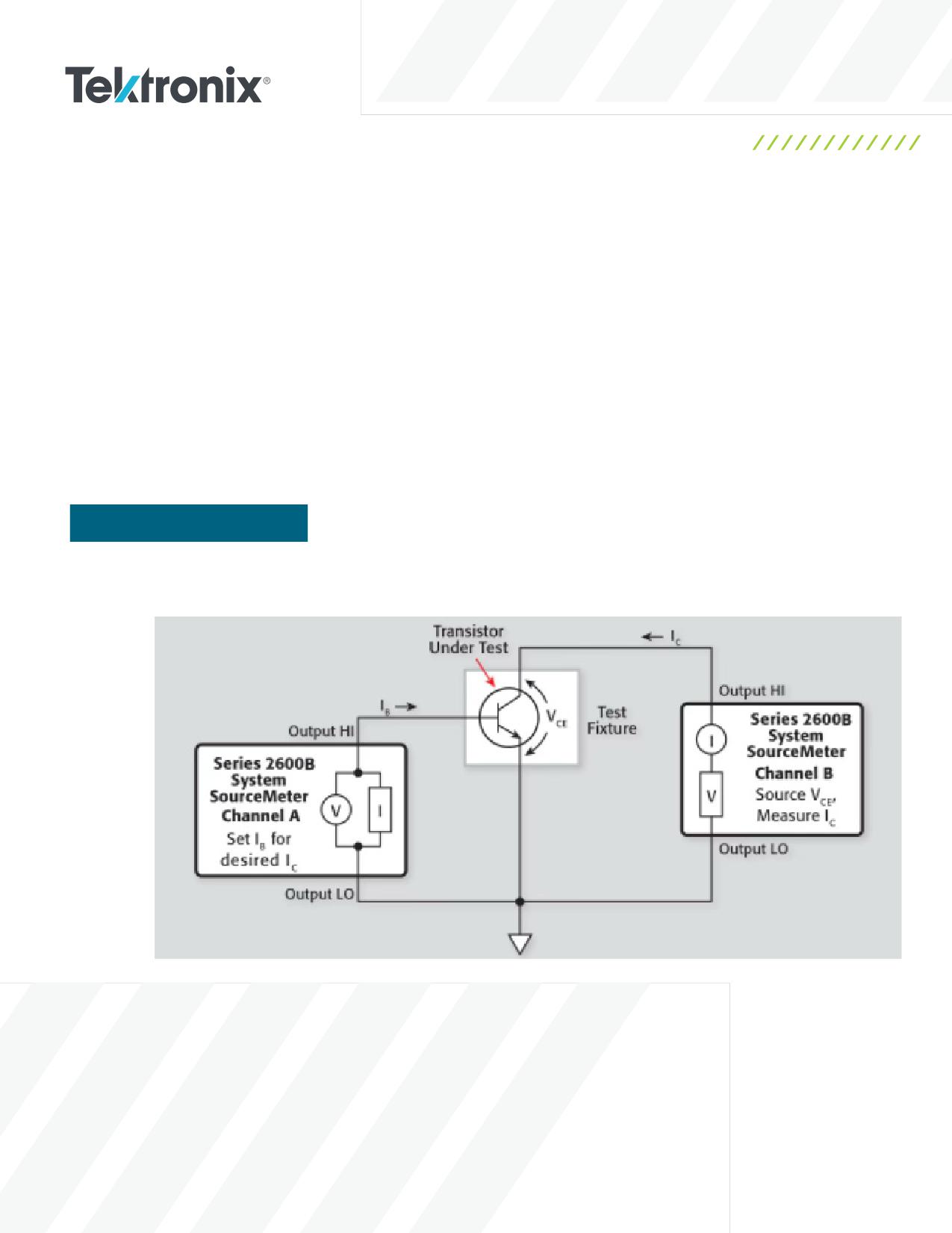
Channel A forces current at the transistor’s base (IB)
amplifiers used in audio systems, wireless communication,
and measures the resulting voltage between the base
or industrial automation, may require “matched”
and emitter (VBE), while channel B forces voltage at the
transistors. Transistor matching guarantees that two or
collector (VC) and measures the resulting current (IC) until
more transistors in a circuit will behave identically, which
(ICE) reaches the target value that shows the transistor is
is crucial for minimizing DC offsets and distortions and
operating within the active region. We can then calculate
improving reliability and performance.
the DC current gain with the following formula:
Transistor matching goes beyond simply using two
hFE = IC /I
B
transistors of the same type from the same manufacturer,
as their behavior may differ due to variances within the
It is important to measure hFE in the active region, as it will
device’s specified tolerances. To guarantee that the
begin to lower as the transistor becomes saturated. A low
transistors are matched, we will need to measure and
or zero reading within the active region typically means that
compare each transistor’s DC Current Gain (hFE), which is a
the transistor under test is faulty or damaged in some way.
commonly used criteria for matching.
For the purposes of this application note, we will be testing a
Tektronix’s KickStart software IV Characterizer App
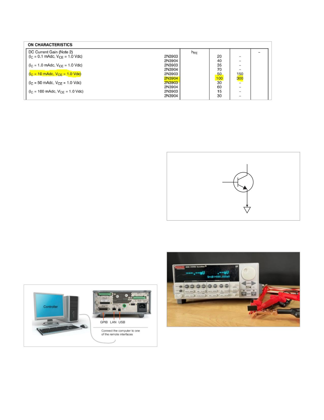
2N3904 BJT. As noted by the table in Figure 2, the required
simplifies instrument control and makes testing BJTs with
current that must be sourced to the base terminal is
two-channel SMUs easy!
between 33 µA and 100 µA for an in spec 2N3904, where:
Figure 1: Diagram visualizing the dual channel model for BJT testing.
2 | WWW.TEK.COM
How to Perform DC Current Gain Testing on Bipolar Junction Transistors
with a Two-channel SMU
APPLICATION NOTE
Figure 2: 2N3904 datasheet table with the nominal on characteristics highlighted.
At a DC current gain of 300 and collector current IC = 10 mA,
Device Connections
the expected base current is
Connect your BJT transistor to the 2602B SMU as shown in
IB = 33 µA
the diagram below:
At a DC current gain of 100 and collector current IC = 10 mA,
Channel B HI
the expected base current is
C
IB = 100 µA
B
Channel A HI
Measuring DC Current Gain of a BJT
E
with KickStart
Channel A+B LO
The KickStart Software IV Characterizer app allows you to
configure a 2602B SMU to test transistors without needing
to interact with the front panel or write any code. KickStart
Figure 4: Device Connections for the test.
also has built in data visualization and export tools, making
it easy to find a matched hFE between two transistors.
For the connections you can use a test fixture or test
leads as shown:
Remote Connections
The remote connections for a 2602B SMU are located on the
instrument’s rear panel. Each series 2600B SMU has access
to remote communications via GPIB, USB, or LAN.
Figure 5: A 2N3904 BJT connected to a 2602B SMU with test leads.
Figure 3: 2602B remote interface connections.
WWW.TEK.COM | 3
How to Perform DC Current Gain Testing on Bipolar Junction Transistors
with a Two-channel SMU
APPLICATION NOTE
Launch KickStart and Set Up the Test
Once you have connected your SMU to your controlling PC, launch the KickStart software and open the IV Characterizer app.
Once the app has launched, apply the settings for channel A (base), channel B (collector), and the common test settings as
shown in Figures 5, 6, and 7. Default settings that remain unchanged will not be called out.
1.
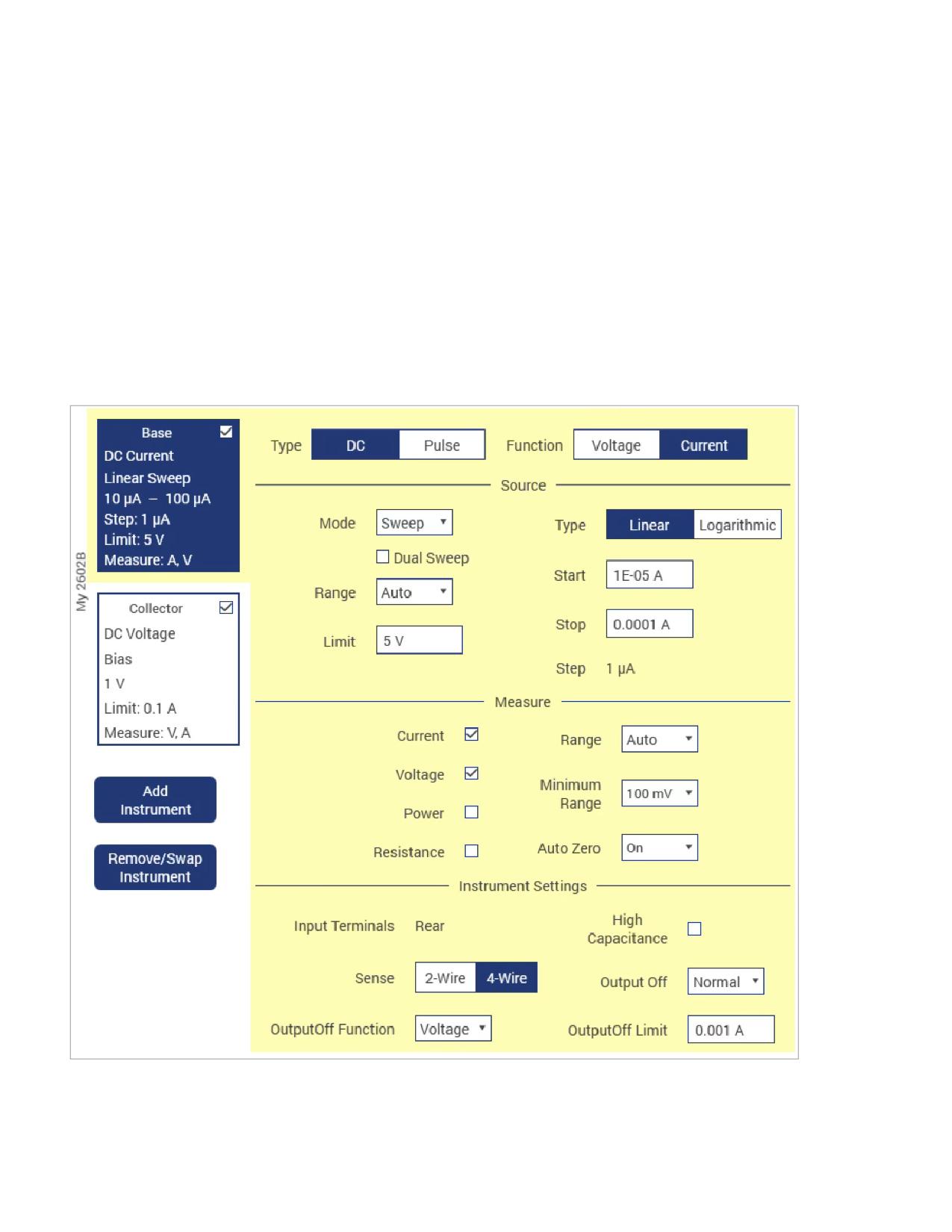
Channel A/ Base Terminal Settings (illustrated in Figure 6):
a. Set the Type to DC.
b. Set the Function to Current.
c. Set the Mode to Sweep.
d. Set the Start level to 10 µA.
e. Set the Stop level to 100 µA.
f. Set the Sense to 4-Wire.
Figure 6: Output settings to configure channel A, which is connected to the transistor base.
4 | WWW.TEK.COM
How to Perform DC Current Gain Testing on Bipolar Junction Transistors
with a Two-channel SMU
APPLICATION NOTE
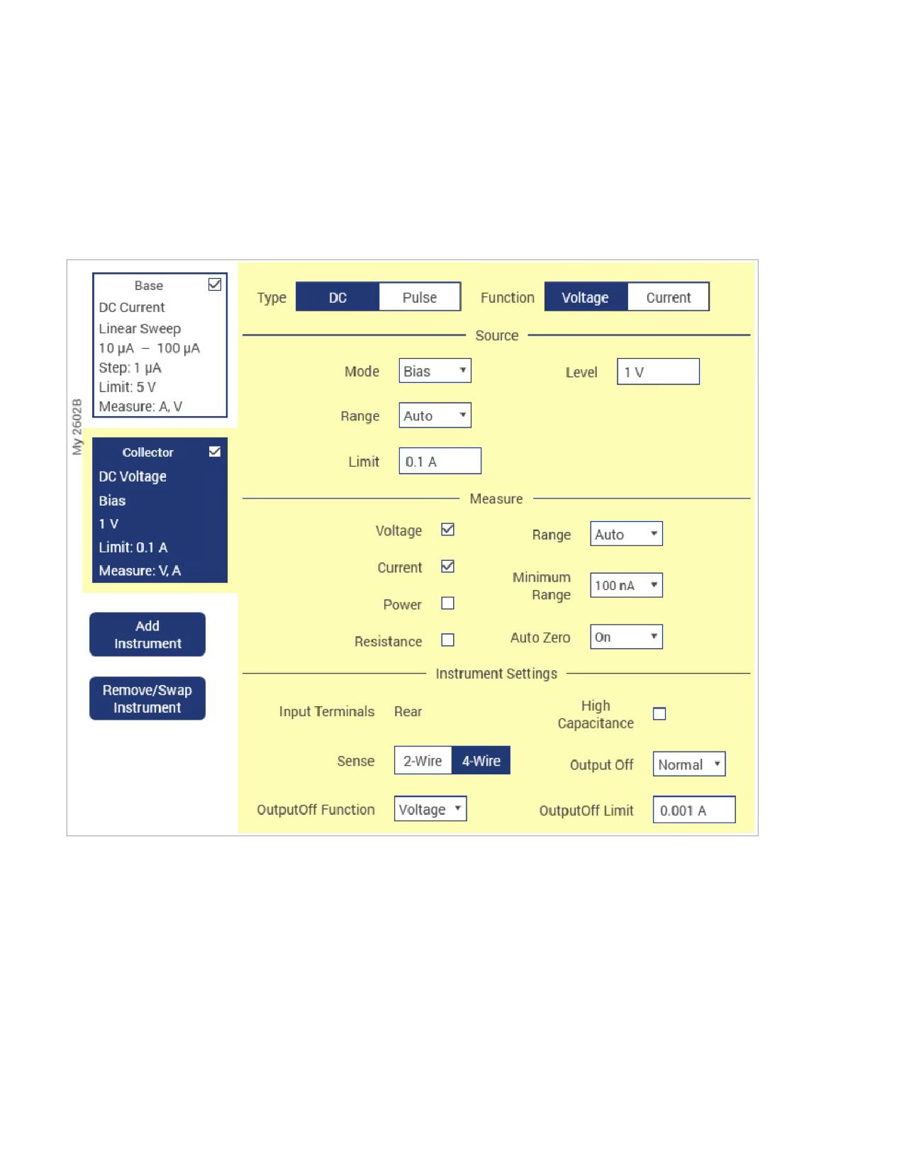
2. Channel B/ Collector Terminal Settings (illustrated in Figure 7):
a. Set the Type to DC.
b. Set the Function to Voltage.
c. Set the Mode to Bias.
d. Set the Level to 1 V.
e. Set the Sense to 4-Wire.
Figure 7: Output settings to configure channel B, which is connected to the transistor collector.
WWW.TEK.COM | 5
How to Perform DC Current Gain Testing on Bipolar Junction Transistors
with a Two-channel SMU
APPLICATION NOTE
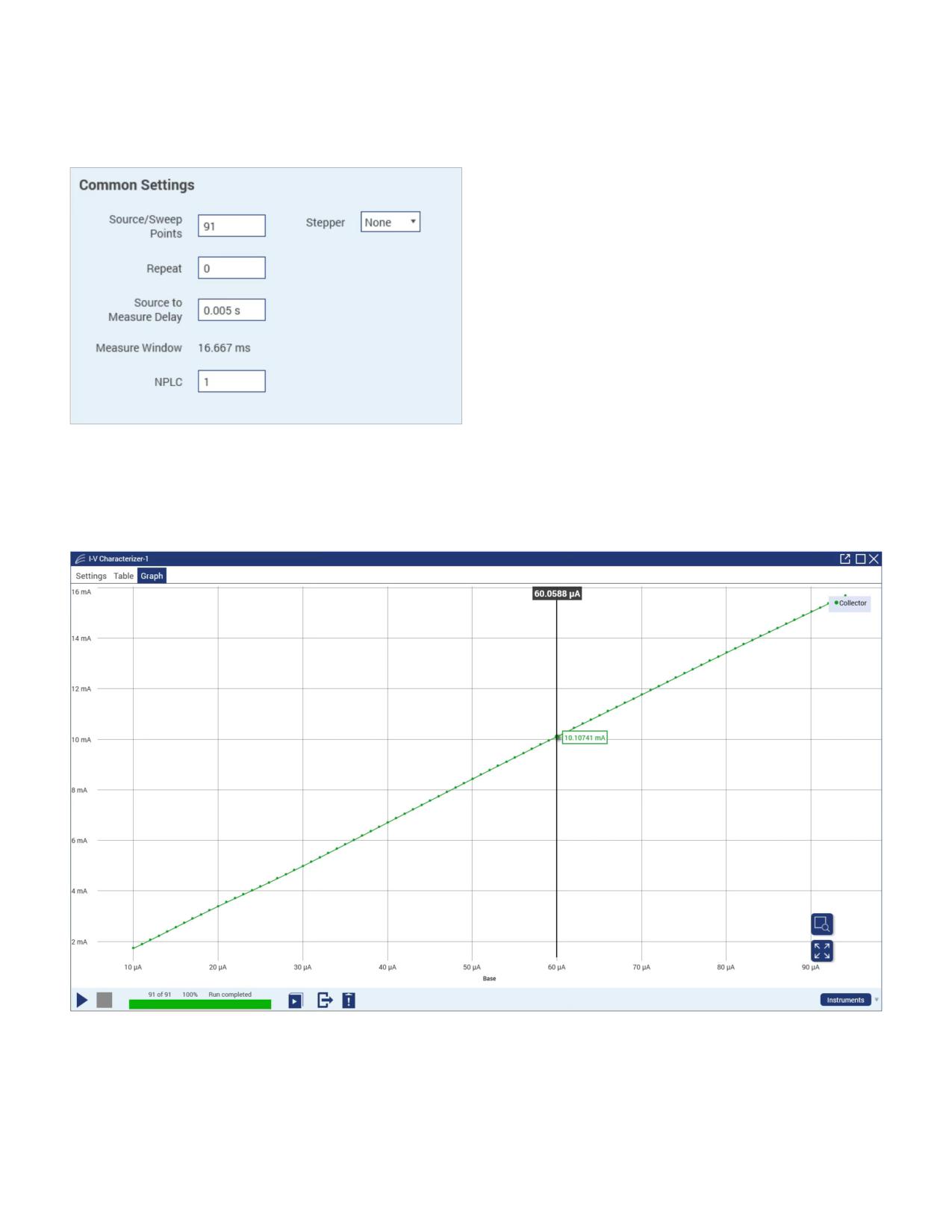
3. The Common Settings (illustrated in Figure 8):
Results
a. Set the Source/Sweep Points to 91.
When the test has finished running, the data can be viewed
in the Table and Graph Tabs.
hFE can be determined by viewing the Graph Tab and setting
the X-axis source to the Base current. Then, find the point in
the graph where the collector current (IC) is 10 mA, and place
a cursor by right clicking in the graph window. The value
reported by the placed cursor will be the measured base
current value (IB).
To calculate the hFE ratio, divide the collector current value
by the base current value:
hFE = IC / IB
Figure 8: The common settings for both channels.
hFE = 10 mA / 60 µA = 166.67
Once all of the settings have been applied, press the run
button to start the test.
Figure 9: The cursor is placed where the collector current reaches 10 mA. The cursor value, 60 µA is the transistor’s base current (IB).
6 | WWW.TEK.COM

How to Perform DC Current Gain Testing on Bipolar Junction Transistors
with a Two-channel SMU
APPLICATION NOTE
Conclusion
Using the 2602B SMU with the KickStart IV Characterizer
app provides a simple and reliable way to measure BJT DC
current gain (hFE) for device evaluation and matching. By
sweeping base current and monitoring collector current
in the transistor’s active region, the setup enables quick
identification of transistors that meet required gain
characteristics. KickStart’s built-in visualization tools
make it easy to locate the IC = 10 mA operating point and
calculate the corresponding hFE, streamlining the process
of selecting well-matched devices.
WWW.TEK.COM | 7

Contact Information:
Australia 1 800 709 465
Austria* 00800 2255 4835
Balkans, Israel, South Africa and other ISE Countries +41 52 675 3777
Belgium* 00800 2255 4835
Brazil +55 (11) 3530-8901
Canada 1 800 833 9200
Central East Europe / Baltics +41 52 675 3777
Central Europe / Greece +41 52 675 3777
Denmark +45 80 88 1401
Finland +41 52 675 3777
France* 00800 2255 4835
Germany* 00800 2255 4835
Hong Kong 400 820 5835
India 000 800 650 1835
Indonesia 007 803 601 5249
Italy 00800 2255 4835
Japan 81 (3) 6714 3086
Luxembourg +41 52 675 3777
Malaysia 1 800 22 55835
Mexico, Central/South America and Caribbean 52 (55) 88 69 35 25
Middle East, Asia, and North Africa +41 52 675 3777
The Netherlands* 00800 2255 4835
New Zealand 0800 800 238
Norway 800 16098
People’s Republic of China 400 820 5835
Philippines 1 800 1601 0077
Poland +41 52 675 3777
Portugal 80 08 12370
Republic of Korea +82 2 565 1455
Russia / CIS +7 (495) 6647564
Singapore 800 6011 473
South Africa +41 52 675 3777
Spain* 00800 2255 4835
Sweden* 00800 2255 4835
Switzerland* 00800 2255 4835
Taiwan 886 (2) 2656 6688
Thailand 1 800 011 931
United Kingdom / Ireland* 00800 2255 4835
USA 1 800 833 9200
Vietnam 12060128
* European toll-free number. If not
accessible, call: +41 52 675 3777
Rev. 02.2022
Find more valuable resources at TEK.COM
Copyright © Tektronix. All rights reserved. Tektronix products are covered by U.S. and foreign patents, issued and pending. Information in this publication supersedes that
in all previously published material. Specification and price change privileges reserved. TEKTRONIX and TEK are registered trademarks of Tektronix, Inc. All other trade names
referenced are the service marks, trademarks or registered trademarks of their respective companies.
032626 SBG 1KW-74237-0