Measuring low resistances (1Ω and lower) has a variety of technical challenges. Depending on the application, test system builders can choose from various instrument options, including a nanovoltmeter used with a current source (for measurements as low as of tens of nano-ohms) or a digital multimeter (DMM) optimized for low-resistance measurements (as low as tens of micro-ohms).
Low-resistance measurements are subject to many of the same sources of error as low-voltage measurements, including offset voltages due to thermoelectric EMFs, offsets generated by rectification of radio frequency interference (RFI), and offsets in the chosen instrument's voltmeter input circuit. Noise sources that can interfere with low-resistance measurement accuracy include Johnson noise, magnetic fields, and ground loops. Excessive common-mode current (the current that flows between the instrument's LO terminal and chassis or earth ground) can also affect low-resistance measurement accuracy. Low-resistance measurements are subject to error sources such as lead resistance, non-ohmic contacts, and device heating. This white paper will address methods to eliminate or minimize these error sources, as well as other measurement considerations, including dry circuit testing and testing inductive devices.
Conquering lead resistance errors with the four-wire method
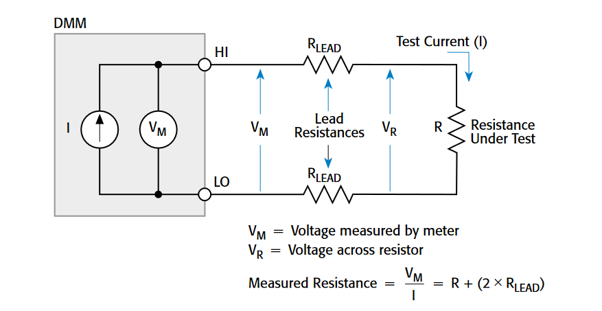
In the two-wire method illustrated in Figure 1, the test current is forced through the test leads and the resistance (R) being measured. The meter then measures the voltage across the resistance through the same set of test leads and computes the resistance value accordingly. Unfortunately, when the two-wire method is applied to low-resistance measurements, the total lead resistance (RLEAD) is added to the measurement. Because the test current (I) causes a small but significant voltage drop across the lead resistances, the voltage (VM) measured by the meter won't be exactly the same as the voltage (VR) directly across the test resistance (R), so considerable error can result. Typical lead resistances are in the range of 10–100mΩ, so it's very difficult to obtain accurate two-wire resistance measurements when the resistance under test is lower than 10-100Ω (depending on lead resistance).
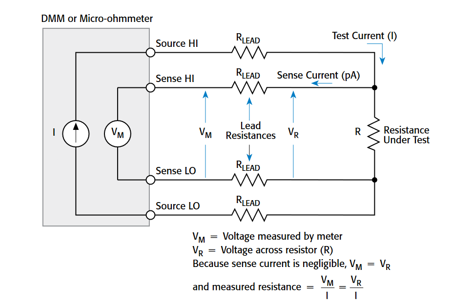
The four-wire (or Kelvin) connection method (Figure 2) is generally preferable for lowresistance measurements. Here, the test current (I) is forced through the test resistance (R) through one set of test leads; the voltage (VM) across the DUT is measured through a second set (the sense leads). The current that may flow through the sense leads is generally small enough to ignore and is not in the voltage measurement portion of the circuit. The voltage drop across the sense leads is also negligible, so the voltage measured by the meter (VM) is essentially the same as the voltage (VR) across the resistance (R). As a result, the resistance can be determined with much greater accuracy. Connect the voltage-sensing leads as close to the resistor under test as possible to avoid including their resistance in the measurement.
Compensating for thermoelectric voltages
Thermoelectric voltages or EMFs are generated when different parts of a circuit are at different temperatures and when conductors made of dissimilar materials are joined together. Several techniques are available to minimize these unwanted offsets.
Current-Reversal Method
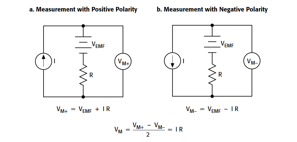
Making two measurements with currents of opposite polarity, as shown in Figure 3, can cancel out thermoelectric EMFs. Note the use of a voltmeter with a separate bipolar current source.With the positive current applied as in Figure 3a, the measured voltage is:
VM+ = VEMF + IR
Reversing the current polarity (Figure 3b) yields the following voltage measurement:
VM- = VEMF - IR
The two measurements can then be combined to cancel thermoelectric EMFs:
| VM = | VM+ - VM- | = | (VEMF + IR) - (VEMF - IR) | = IR |
| 2 | 2 |
The measured resistance is computed in the usual manner:
| R = | VM |
| I |
This completely cancels out the thermoelectric voltage. However, to be effective, a low noise voltmeter with a response speed that is faster than the thermal time constant of the circuit under test is essential. If the response speed is too slow, any changes in the circuit temperature will cause changes in the thermoelectric EMFs that won't be completely canceled, so some error will remain.
Delta Method
If changing EMFs are causing inaccuracies, the delta method may be preferable. Like the current-reversal method, it involves alternating the current source polarity, but it uses three voltage measurements to make each resistance calculation instead of just two.
Figure 4 shows the voltage drop of a DUT as a function of time with an alternating polarity current applied. A voltage measurement (VM1, VM2, VM3, etc.) is taken each time the polarity is changed. Each one includes a constant thermal voltage offset (VEMF) and a linearly changing voltage offset (δV). The thermal voltage drift may be approximated as a linear function over short periods, so the rate of voltage change as a function of time (δV) can also be treated as a constant.
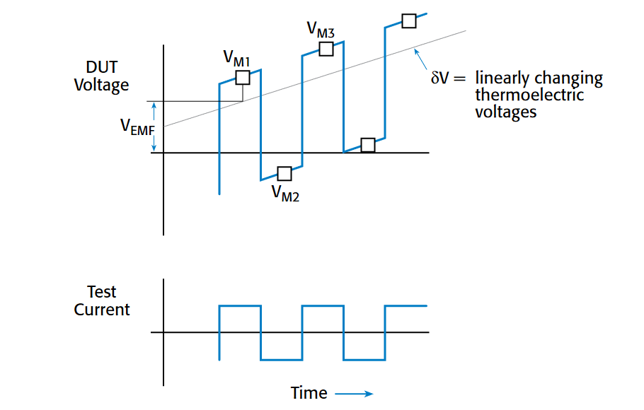
Using three voltage measurements allows canceling out both the thermoelectric voltage offset (VEMF) term and the thermoelectric voltage change (δV) term. In the delta method, each data point is the moving average of three readings. The resulting data has lower noise than the data derived using the current-reversal method, even when both sets of data are taken over the same period. The success of the delta method depends on the linear approximation of the thermal drift, which must be viewed over a short period.
Just as in the current-reversal method, compensating for changing EMFs means the measurement cycle time must be faster than the DUT's thermal time constant, so it's essential to use a fast current source. Typically, a nanovoltmeter is used to obtain the necessary low voltage sensitivity. For a detailed exploration of this offset compensation technique, consult Keithley's "Achieving Accurate and Reliable Resistance Measurements in Low Power and Low Voltage Applications."
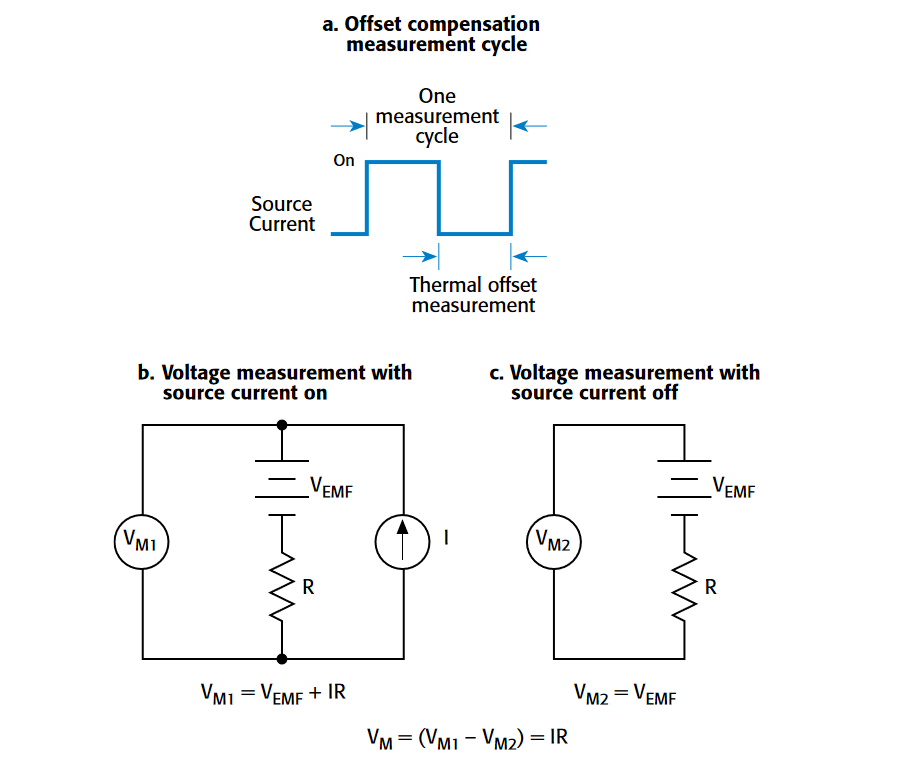
Offset-Compensated Ohms Method
This method is similar to the current-reversal method except the measurements are alternated between a fixed source current and zero current. As shown in Figure 5a, the source current is applied to the resistance being measured during only part of the cycle. When the source current is on, the total voltage measured by the instrument (Figure 5b) includes the voltage drop across the resistor as well as any thermoelectric EMFs, and it is defined as:
VM1 = VEMF + IR
During the second half of the measurement cycle, the source current is turned off and the only voltage measured by the meter (Figure 5c) is any thermoelectric EMF present in the circuit:
VM2 = VEMF
Given that VEMF is accurately measured during the second half of the cycle, it can be subtracted from the voltage measurement made during the first half of the cycle, so the offsetcompensated voltage measurement becomes:
VM = VM1 - VM2
VM = (VEMF + IR) – VEMF
VM = IR
and,
| R = | VM |
| I |
Again, note that the measurement process cancels the thermoelectric EMF term (VEMF)
Non-Ohmic Contacts
Non-ohmic contacts are evident when the potential difference across the contact isn't linearly proportional to the current flowing through it. They may occur in a low-voltage circuit as a result of oxide films or other non-linear connections and are likely to rectify any radio frequency energy (RFI) present, leading to the appearance of an offset voltage in the circuit
If measuring low resistances with a DMM, change the measurement range, which will usually change the level of test current as well. The same reading but with higher or lower resolution (depending on whether the instrument was up- or down-ranged) will indicate a normal condition. However, a reading that's significantly different may indicate a non-ohmic condition.
When using a separate current source and voltmeter to make low-resistance measurements, check both instruments for non-ohmic contacts. If the current source's contacts are non-ohmic, here may be a significant difference in the compliance voltage when the source polarity is reversed. If the voltmeter's contacts are non-ohmic, they may rectify any AC pickup present and cause a DC offset error. If this is the case, the offset-compensated ohms method is preferable to the current-reversal method for canceling offsets.
To prevent non-ohmic contacts, choose an appropriate contact material, such as indium or gold, and make sure the compliance voltage is high enough to avoid problems due to source contact non-linearity. To reduce error due to voltmeter non-ohmic contacts, use shielding and appropriate grounding to reduce AC pickup
Device Heating
Device heating can be a consideration when measuring the resistance of temperature-sensitive devices such as thermistors. The test currents used in low-resistance measurements are often much higher than those used for high-resistance measurements, so the resulting power dissipation and temperature increase in the device can cause the device's resistance to change
Most DMMs don't provide the means for setting the test current level; it is generally determined by the measurement range. Therefore, some alternate means must be found to minimize device heating. One simple but effective way to do so is to use the instrument's one-shot trigger mode, in which the instrument applies only a single, brief current pulse to the DUT during the measurement cycle, minimizing device-heating errors. Offset compensation could also be used to reduce device heating. In offset compensation, the test current is applied for only 50 percent of the total test time, thereby reducing the power through the DUT.
Low-Resistance Measurement Applications
Some of the most common types of low-resistance measurement applications include inductive device testing, measurements of contact resistance and superconductor resistance, and resistivity measurements of conductors. These measurements can be made with a nanovoltmeter with a current source.
Testing Inductive Devices
Inductive devices usually have a small resistance in addition to the inductance. This small resistance is normally measured with a DMM, but the interaction between the inductance and the measuring instrument can complicate these measurements. Some of the problems may include oscillations, negative readings and generally unstable readings.
When problems occur, try to take measurements on more than one range and check if the values correspond. If possible, avoid using offset compensation (pulsed current) because inductive reaction to the current pulse may cause unstable measurements or make autoranging difficult. Try using a higher resistance range when possible
Check for oscillations by connecting an oscilloscope in parallel with the device and the meter. Sometimes, a diode across the inductor may settle down the oscillations by clamping the inductive kickback voltage when the field collapses.
Contact Resistance Measurements
Contact resistance is the resistance to current flow through a closed pair of contacts. These measurements are made on components such as connectors, relays, and switches, and normally range from micro-ohms to a few ohms. Typically, an ohmmeter with fourterminal measurement capability is used to prevent lead resistance from being added to the measurement.
Often, the purpose of the contact resistance test is to determine whether contact oxidation or other surface film buildup has increased the DUT's resistance. If the voltage across the device is too high, the film will be ruptured, invalidating the test. The level of voltage required to break down a film usually ranges from 30 to 100 millivolts.
Excessive current through the contacts during testing can soften or melt the contact points and the surrounding area, enlarging the contact area, and reducing the contact resistance. The dry circuit method is usually used to prevent these problems. A dry circuit is a technique in which the voltage and current are limited to levels that can't cause changes in the physical and electrical condition of the contact junction. In general, that means the open circuit voltage is 20 millivolts or less and the short circuit current is 100 milliamps or less. Because of the low test current level, a very sensitive voltmeter is required to measure the voltage drop, which is usually in the microvolt range. Other test methods create the potential for physical or electrical changes to the contact, so dry circuit measurements should be made before any other electrical tests.
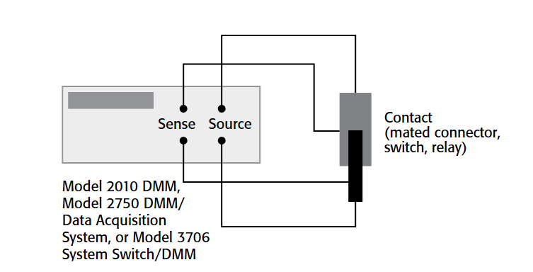
Figure 6 illustrates making four-wire contact resistance measurements with a Model 2010 DMM, Model 2750 DMM/Data Acquisition System, or Model 3706 System Switch/DMM. These instruments can automatically compensate for thermoelectric offsets in the sense circuit by using the offset compensation mode. They also have built-in dry circuit measurement capability. For most applications, a DMM with an extended ohms measurement range is sufficient for contact resistance measurements, but if the short circuit current or measured resistance values are much smaller than the DMM's specifications, use a nanovoltmeter/current source combination instead.
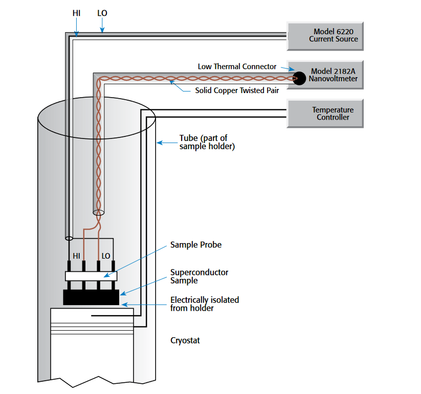
Superconductor Resistance Measurements Some materials lose their resistance to electrical current and become superconductive at extremely low temperatures. A superconductor's transition temperature (the point at which its resistance changes from a finite value to zero) and critical current density (the maximum current density it can carry under specific temperature and magnetic field conditions before becoming resistive) are two commonly measured parameters. Characterizing these parameters requires measuring very small resistances.
Figure 7 shows a basic superconductor resistance measurement configuration. The voltage leads should be made of a material with a low Seebeck coefficient with respect to the sample. A nanovoltmeter is crucial to obtaining precision measurements. For transition temperature measurements, the current source must be kept below the sample's critical current. If the current becomes too high, the power dissipated may damage the sample and the cryostat. For critical current measurements, however, the current source must be able to exceed the critical current of the sample. The current source should have programmable polarity, so the test can be performed using the current-reversal method.
In recent years, instrument manufacturers have developed a number of functions that simplify the measurement process. For example, Keithley's Model 2182A Nanovoltmeter and Model 6220 Current Source are designed to work together to implement the delta method automatically. In this mode, the Model 6220 automatically alternates the polarity, then triggers the nanovoltmeter to take a reading at each polarity. Then, the current source displays the "compensated" resistance value. The resistance can be plotted vs. temperature as the sample temperature is changing. For determining the critical current, the nanovoltmeter and current source can be used together to produce a precision I-V curve over a range of currents.
Resistivity Measurements of Conductive Materials
The resistivity of a conductor is determined by measuring the resistance of a sample of known geometry by forcing a current through the sample with one pair of leads while measuring the voltage drop with a second pair of leads. Although the specific method for determining the resistivity depends on the size and shape of the sample, all methods require a sensitive voltmeter with a current source.
Resistivity of Bulk Materials
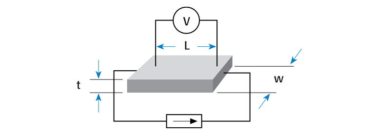
Figure 8 illustrates a system for testing the resistivity of a bulk material such as a metal bar or rod. The current source is connected to both ends of the sample. The voltmeter leads are placed a known distance apart. The resistivity is calculated from the cross-sectional area of the sample and the distance between the voltmeter leads:
| ρ = ( | V | ) | ( | A | ) |
| I | L |
where ρ = resistivity in ohm-cm, V = voltage measured by voltmeter, I = source current, A = cross sectional area of sample (w × t) in cm2, and L = length of distance between voltmeter leads in cm.
To compensate for thermoelectric voltages, one voltage reading is taken with positive test current and another taken with negative current. The absolute values of these two readings are then averaged and used in the equation for V/I. Most materials have a significant temperature coefficient, so be certain to maintain the sample at a known temperature.
van der Pauw Method
Although van der Pauw resistivity measurements are used primarily in the semiconductor industry, they have other applications, such as determining the resistivity of superconductors or foil. The van der Pauw method is used on samples that are flat, uniformly thick, and arbitrarily shaped, and that do not contain any isolated holes. The contacts used should be small and placed on the periphery of the sample. Eight measurements are made around the sample; these readings are combined mathematically to determine the average resistivity of the sample.
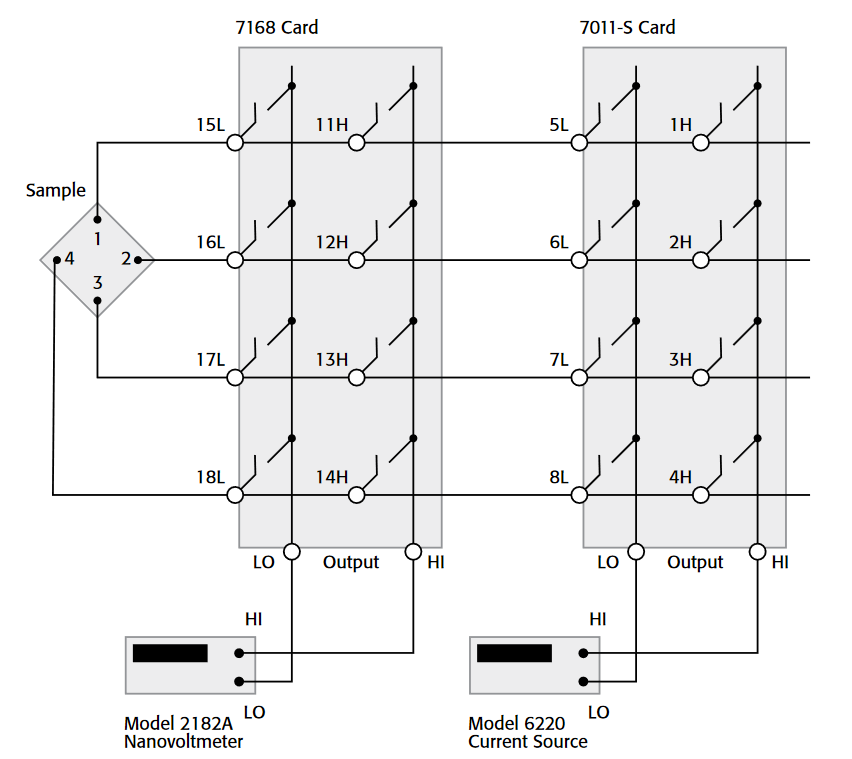
Figure 9 illustrates a configuration useful for determining the resistivity of a conductive sample using the van der Pauw method. It includes a Model 6220 Current Source to supply the current through the sample and a Model 2182A Nanovoltmeter to measure the resulting voltage drop.
Summary
As this article outlines, the right combination of instrumentation and measurement techniques can go a long way toward ensuring the accuracy of low-resistance measurement applications. For more tips and techniques on making better low-resistance measurements, click here to download a free copy of Keithley Instruments 244-page Low Level Measurements Handbook.
Find more valuable resources at TEK.COM
Copyright © Tektronix. All rights reserved. Tektronix products are covered by U.S. and foreign patents, issued and pending. Information in this publication supersedes that in all previously published material. Specification and price change privileges reserved. TEKTRONIX and TEK are registered trademarks of Tektronix, Inc. All other trade names referenced are the service marks, trademarks or registered trademarks of their respective companies.
No.3086 7.23.10