Serial Data Network Analysis (SDNA) Application
The transition in computer, communications, and consumer electronics industries from parallel to high-speed serial data is creating new design challenges. As more data bits must pass through the same interconnect link, the data rates are pushed higher into multi gigabit regime, creating substantially tighter timing budgets. Higher data rates also create more inter-symbol interference (ISI) due to highfrequency losses in the interconnects. Additionally, to allow designers to achieve even higher data transfer rates, several of these serial links are commonly used at the same time, creating what is referred to as multilane configuration, where crosstalk again plays an important role. As a result, characterization of interconnect reflections, losses and cross-talk must be managed more closely. This characterization must be done differentially, and is done more and more often in frequency rather than in time domain, using so-called S-parameters (see Appendix A – S-parameter Backgrounder). S-parameters give you quantitative insight into causes of bit errors and bit error rate (BER) degradation, jitter, ground bounce, and EMI. Crosstalk can also be done as an S-parameter measurement, looking at signal transfer from one line pair to the adjacent one. Many electrical standards – such as SATA, PCI Express, FibreChannel and Gigabit Ethernet to name just a few – now require S-parameters in their compliance test procedures. The differential serial data compliance testing and differential characterization of serial data components can be jointly described as Serial Data Network Analysis (SDNA).
Traditional tools for S-parameter measurements commonly referred to as Vector Network Analyzers (VNA). These tools tend to be very powerful – but that power may very well be their own undoing, as their accuracy is achieved through extensive calibration procedures. For SDNA applications, these differential calibration procedures are excruciatingly lengthy and difficult to follow, resulting in lengthy test times and being prone to human error. Electronic calibration modules for VNAs are available, but operate only at relatively low frequencies for most SDNA applications. Additionally, the cost of the VNA instruments tend to be high compared to an average instrument that a digital designer would have on their workbench.
TDR-based S-parameter measurement tools (see Appendix B – TDR-based S-parameter Measurements) are proven to be cost effective, easy to use, easy to calibrate, highly accurate, and provide higher throughput. For example, one can obtain a differential insertion loss measurement with TDR and post-processing software within a minute instead of the 15 minutes or so typically required by a VNA. VNAs also can not measure directly to DC, they can take a long time to accurately measure low frequencies for long DUTs such as cables, and they compute the differential response of the system from single ended measurement rather than measure it directly. A TDR-based system can measure DC and low frequencies directly, and Tektronix' DSA8200 and IConnect ® S-parameter measurement system can obtain true differential TDR and S-parameters directly by firing more than one source simultaneously – a unique capability of this kind in the industry. IConnect also allows acquisition of extremely long records (up to 1,000,000 points), which is required for making S-parameter measurements for very long devices such as cables. Finally, the typical cost of a TDR-based system can easily be 1/2 the cost of a comparable VNA system – and the VNA system will provide lower time domain resolution than the TDR with comparable bandwidth. There are several misconceptions about TDRbased S-parameters, which are clarified in Appendix C – Misconceptions about TDR-based S-parameters. Overall, a TDR-based S-parameter measurement system provides a high throughput and easy-to-use approach to performing S-parameter compliance tests required by many digital standards, as well as for characterization of digital devices operating at gigabit speeds.
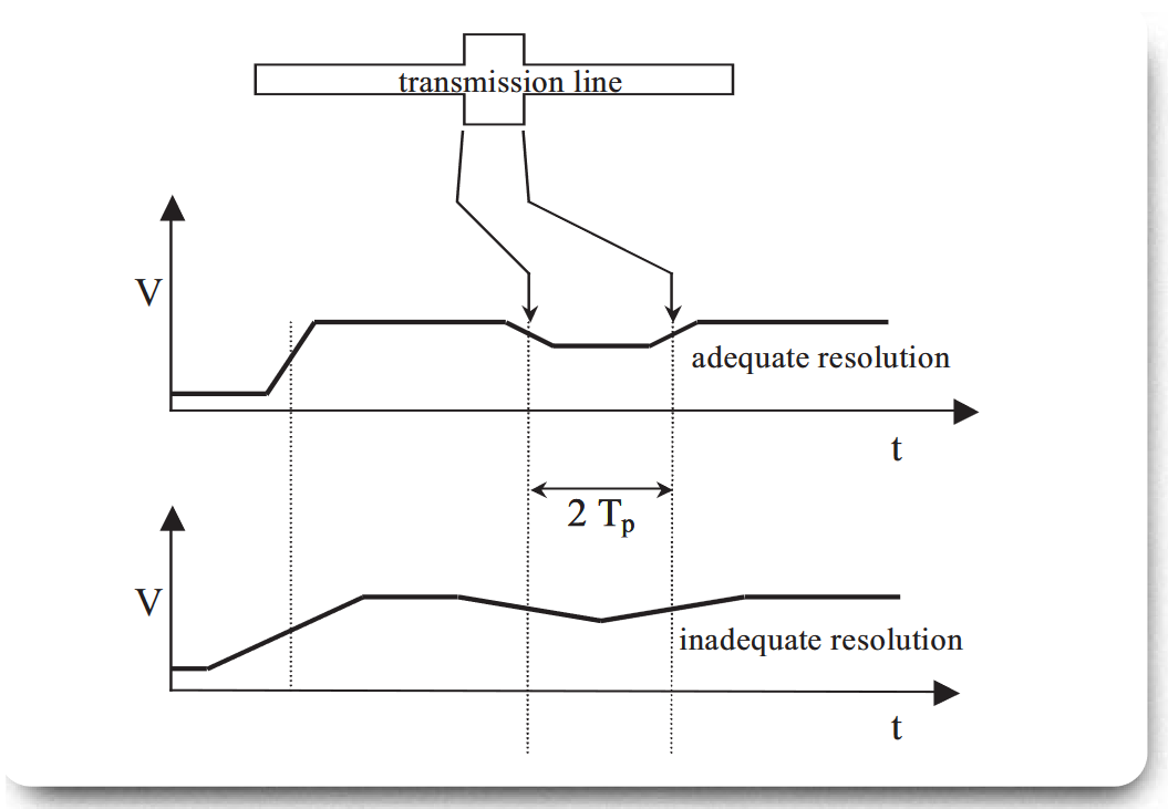
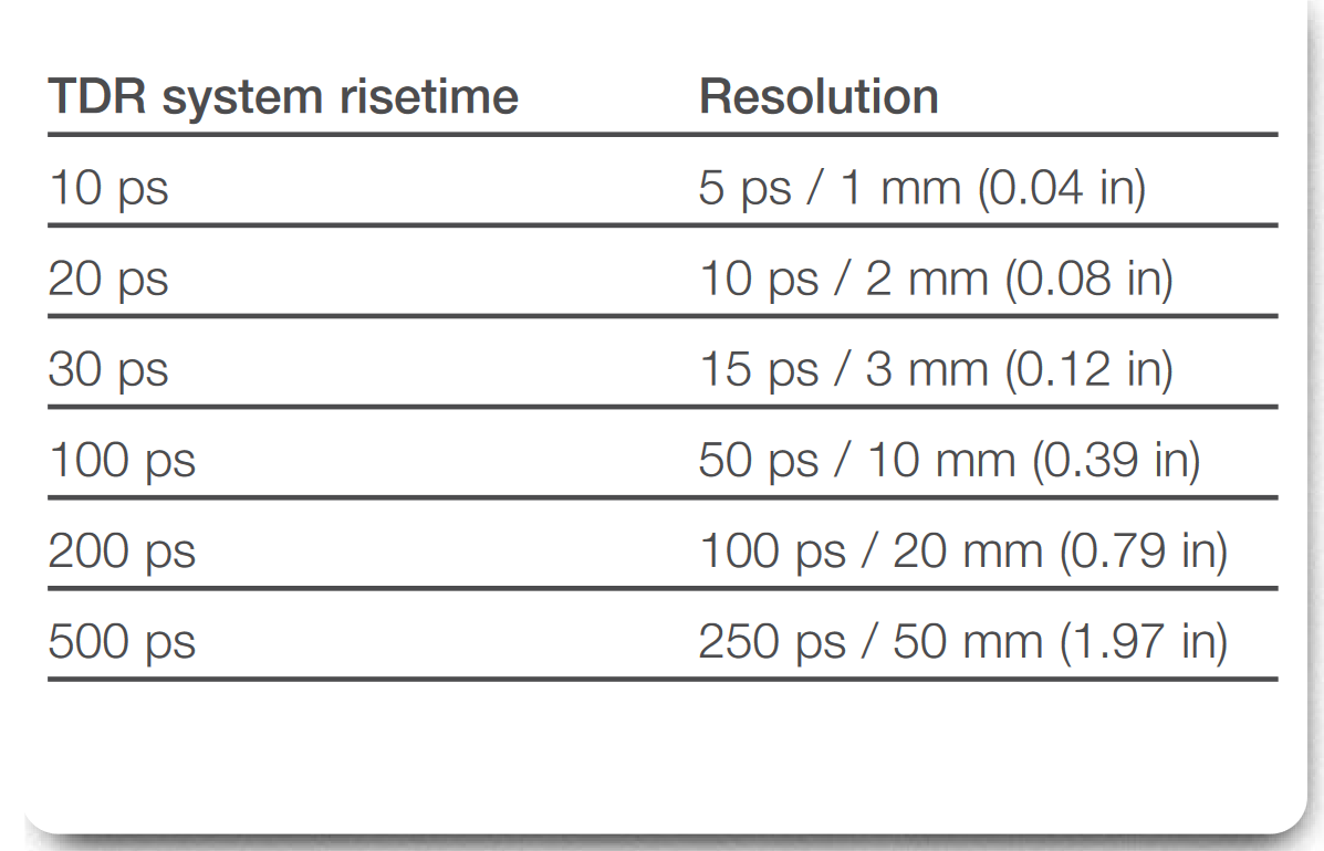
Let's start with the most basic requirement for TDR, which is to provide sufficient resolution for locating faults in a package or a circuit board. The Institute for Printed Circuits (IPC) TM-650 2.5.5.7 document defines TDR resolution as “the resolution limit … wherein two discontinuities or changes on the transmission line … begin to merge together … Per this definition, the resolution limit is: half the … 10% to 90% risetime or 90% to 10% fall time (depending on whether the TDR response is calibrated with a short or open circuit).” For typical surface microstrips in the air, and on FR4 circuit boards (Vp ≈ 2x10⁸ m/s), the resolution and TDR rise time requirements are summarized in IPC TM-650 using the preceeding table.
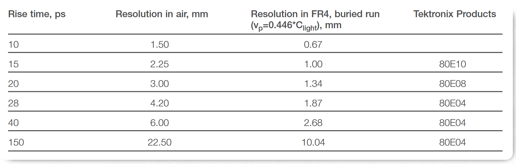
An inner board layer (a stripline) is much more representative of the typical board run. Additionally, it is useful to provide the resolution data for propagation in free air. For stripline, we assume Vp = 0.446xclight=1.34x10⁸, and the resulting resolution data, based on the rule of tTDR/2, is summarized in Table 2 above.
Let's look at a practical situation. On the Tektronix TDR demonstration board, there are resolution structures that are reasonably close to the 2.4 mm (S) connector on the board (Figure 2).
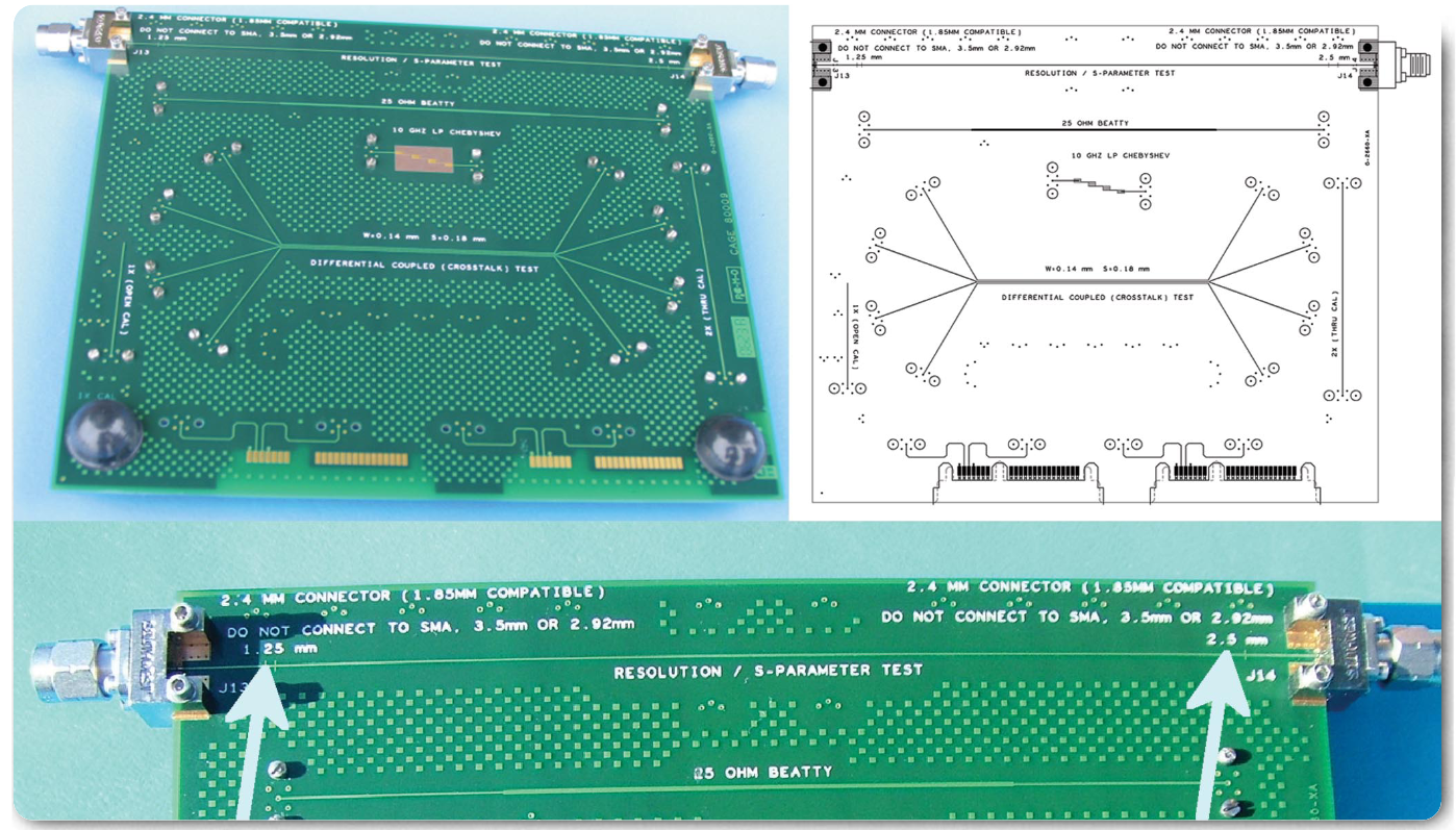
Figure 3 presents the results of TDR testing using the Tektronix 80E10 15 ps reflected rise time TDR module, with the signal launched from the left to access 1.25 mm structure, and the signal launched from the right to access 2.5 mm structure.
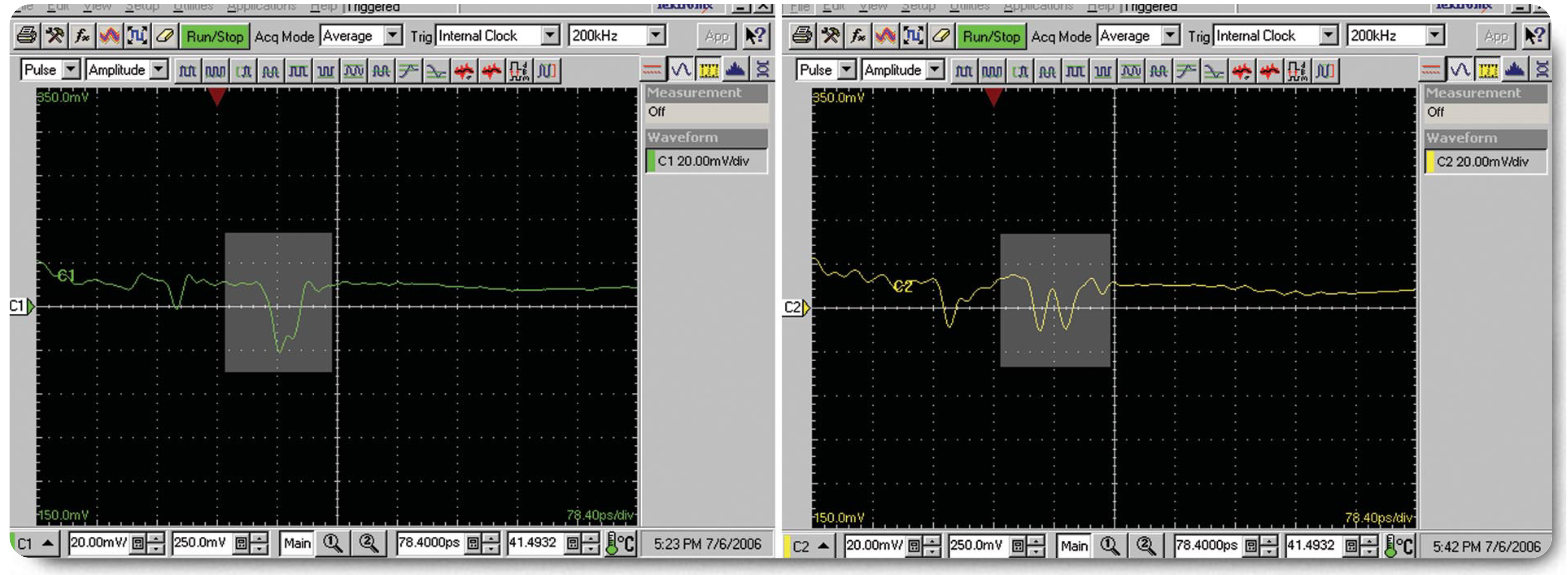
Clearly, on the structure with 2.5 mm separation, the two discontinuities are resolved perfectly, whereas on the structure with 1.25 mm separation, you start to lose resolution (the trace on the demo board is a microstrip, and according to Table 1 there is a different limit on the resolution for microstrips). The interesting question is, however, what happens for spacing under 1.25 mm between discontinuities.
The discontinuities do not disappear; they simply become one single discontinuity. Clearly then, when a failure analyst attempts to locate a single discontinuity, even a sub-mm discontinuity will be observed by 80E10. This is an important conclusion; sub-mm resolution can be achieved with 15 ps reflected rise time in 80E10 module.
Rise Time Requirements for Serial Standards
When using a TDR-based S-parameter measurement system for characterization or for a compliance test defined by a specific standard, it is important to know what rise time is required to accurately perform measurement or test. When specifying the rise time, standards focus primarily on the maximum (slowest) rise time, looking at the minimum rise time as an informative parameter. SATA test procedures, for example, state the required minimum rise time but then a footnote clarifies that “Failures at minimum rate have not been shown to affect interoperability and will not be included in determining pass/fail for interoperability testing.” So, for most standards the question for a designer remains – what is the TDR rise time do you need for a given specification, given data rate, and given S-parameter bandwidth specified by a standard?
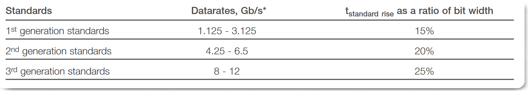
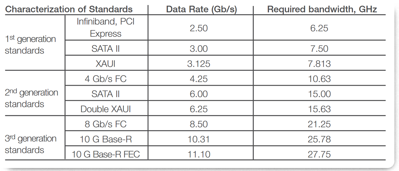
During a recent study of standards at Tektronix, a clear trend has been observed, where rise times for 1st generation standards (e.g., Infiniband SDR, PCI Express etc.) constituted a substantially smaller portion of the bit width (or unit interval) than the 2nd (e.g, Infiniband DDR, PCI Express 2.0, 4 Gb/s FibreChannel) and 3rd (8 Gb/s FibreChannel, 10 Gb/s Ethernet) generation standards. The approximate dividing line between the generations of standards can be drawn at 3.125 for 1st to 2nd generation transition and 6.5 Gb/s for 2nd to 3rd generation transition. We found that the rise time constituted approximately 15% of the bit width for the 1st generation standards, 20% for 2nd generation, and 25% for 3rd generation (all rise times are measured as 20-80%). This information is summarized in the table above.
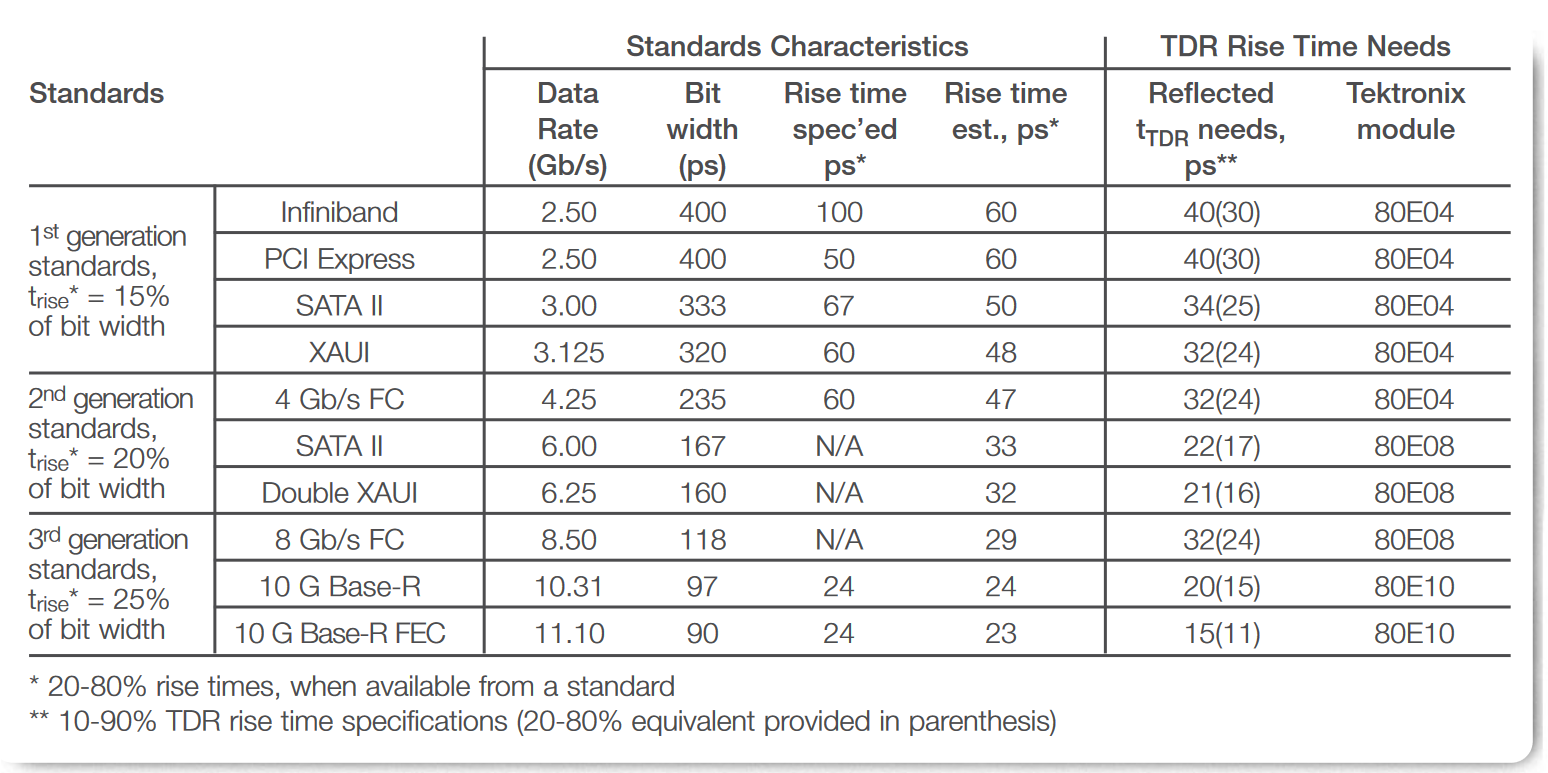
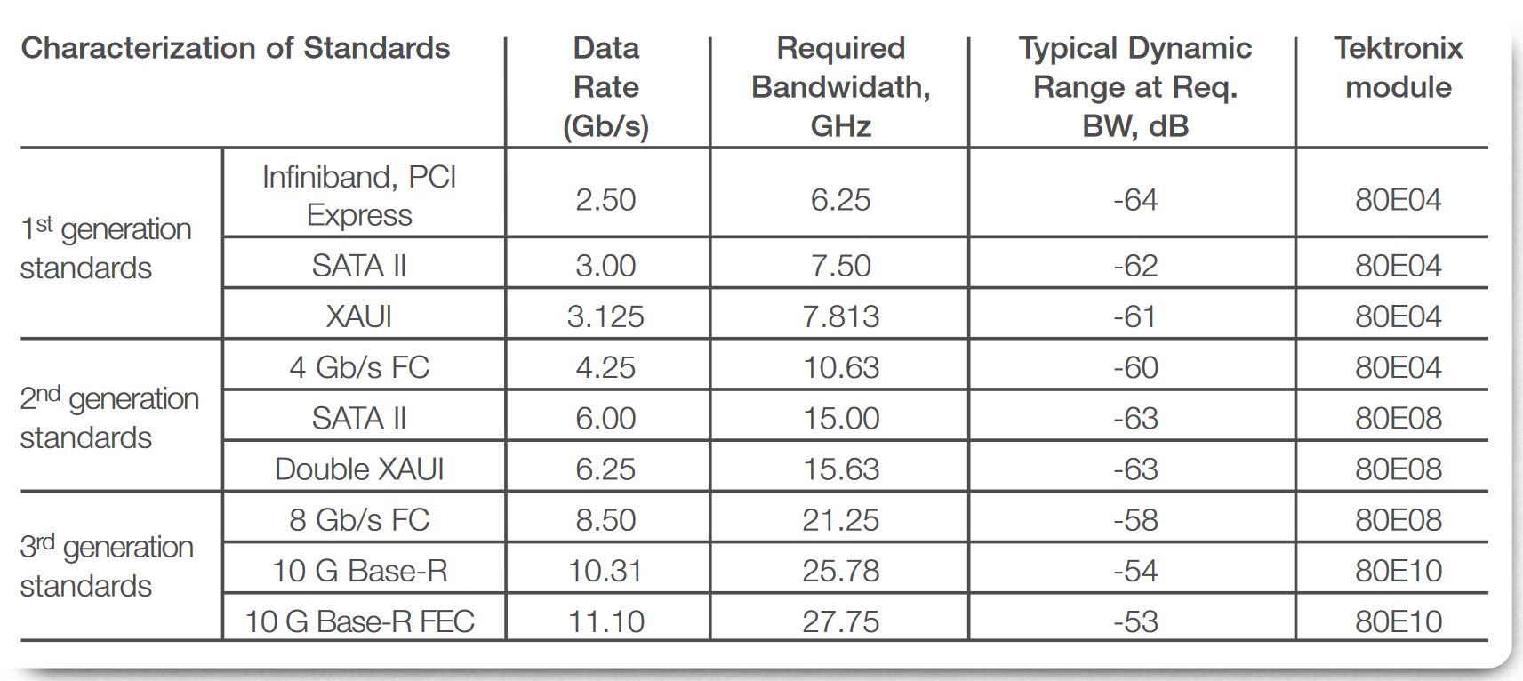
If a designer used TDR rise time that is 50% faster than the rise time used by the devices in various standards, complete characterization of the channel with more than adequate guardband could be achieved (note that TDR rise time is defined in terms of 10-90%, which provides additional guardband over the 20-80% rise time specified by the standards). This assumption ensures that the rise time provided is sufficiently fast for characterization. If the rise time needs to be slowed down, this can be achieved with either mathematical filtering in the oscilloscope, or using sufficiently lossy cables or filters. Using this 50% guardband assumption, the following summary table specifies how much TDR rise time is required by various standards, and what Tektronix modules can address that.
Dynamic Range Requirements for Serial Data
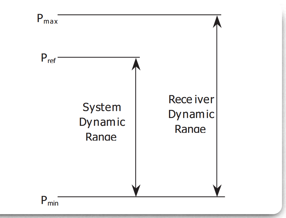
Now let's define dynamic range. Typically, receiver dynamic range is defined in terms of difference between maximum and minimum power that can be measured – Pmax and Pmin (Figure 4). System dynamic range is defined in terms of the difference between the nominal power of the source (Pref) and the minimum power that can be measured (Pmin). In TDR-based S-parameter measurements, Pmax is related to maximum operating spec of a sampling module, and is less relevant when one focuses on the passive component (interconnect) measurements. As a consequence, system dynamic range is what matters for serial data interconnect characterization.
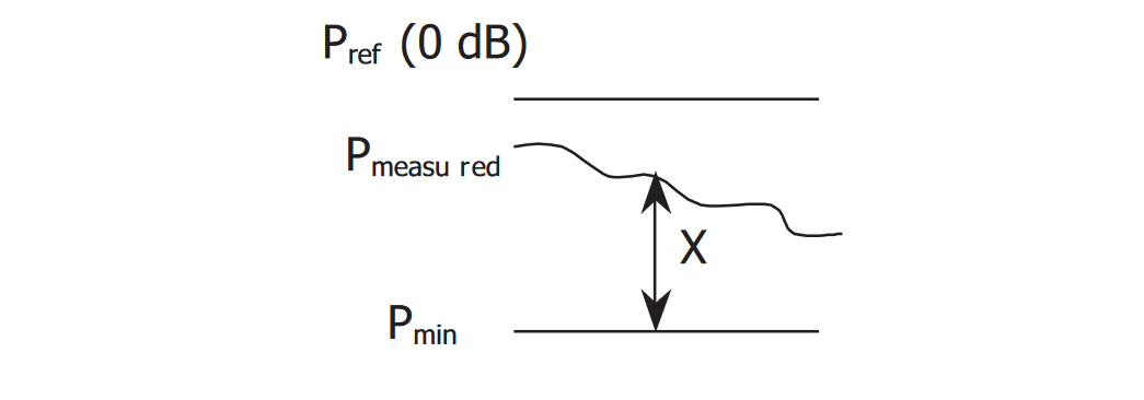
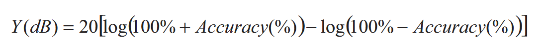
How does this relate to the serial data dynamic range requirements? In essence, per the discussion above, dynamic range is the difference between 0 dB and the noise floor. The actual accuracy of the measurement at a given frequency depends on what is the difference between an actual measurement level (Pmeasured) vs. the noise floor (Pmin). If our actual device under test is measured with the noise floor at X dB below reference measurement level, it can be demonstrated that the accuracy in %, can be related to the X dB below reference value as follows

Note that since the signal and noise in frequency domain add vectorially (equation above shows worst case accuracy) when the noise vector is completely in phase (or 180 degree out of phase) with the signal vector.
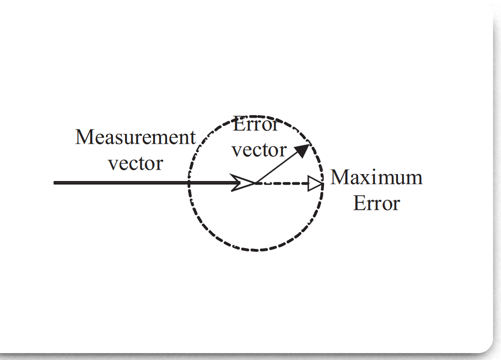
Additionally, it can be demonstrated that total peak-to-peak ripple (error circle diameter in Figure 5) on that signal will be Y dB using the following equation:
This equation includes both the positive and the negative ripple observed on the waveform.
You can now produce the following charts, which demonstrate what accuracy can be achieved depending on how far the dynamic range is below the measurement level. Detailed tables are given in Appendix E – Accuracy vs. Dynamic Range Below Measurement Level.
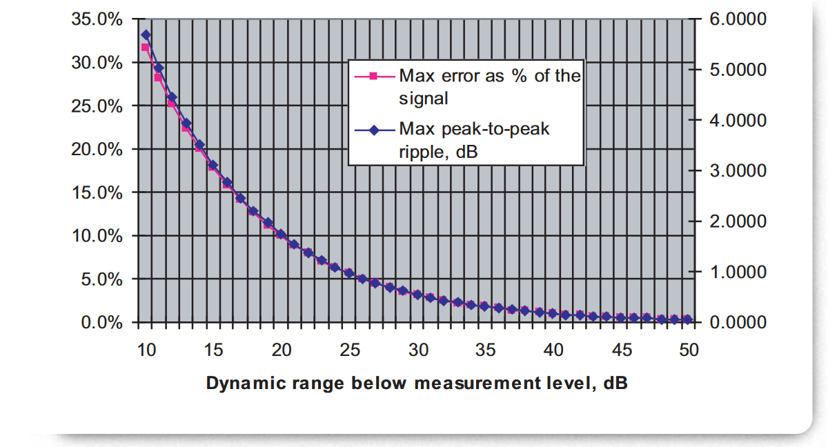

For a typical characterization work in any of the serial data standards, you would want to measure a voltage no smaller than approximately 10% of the full signal amplitude. This voltage glitch can be caused by reflections, or by crosstalk from an adjacent differential line pair. This type of voltage glitch still will provide an 80% eye opening, approximately, as illustrated by Figure 7.
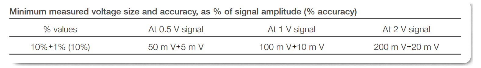
It is adequate to measure this voltage glitch with 10% accuracy (which translates into accuracy that is 1% of the full signal amplitude). This set of typical measurement requirements is summarized in Table 4, and examples are given for translating the percentage into voltage at 500 m V, 1 V, and 2 V peak to peak amplitude signals.
Using the accuracy chart (Figure 6) and the table in Appendix E, it can be determined that a signal that is 10% of total amplitude is -20 dB, and to measure it with 10% accuracy, the noise floor needs to be another -20 dB below the measurement level, making the total dynamic range requirement -40 dB.
Frequency Requirements for Serial Data
Tracking the 1st-2nd-3rd generation division for serial standards discussed above, it was discovered that the later generation of standards place less stringent requirements on characterization of digital components. For the 1st and 2nd generation standards, designers talked about characterization to the 5th harmonic of the clock (even though much lower compliance testing requirements were stated in the standards), and for 3rd generation standards designers talked about the 3rd harmonic.
Overall, performing characterization to the 5th harmonic ensures adequate characterization bandwidth, and provides sufficient confidence to the designer. Using the 5th harmonic as a guideline, Table 5 provides the frequency requirements.

Tektronix TDR Modules Meet the Challenge
Figure 8 is the typical dynamic range for the 80E10 module. Notably, dynamic range degrades with frequency. This is due primarily to step-like nature of the TDR incident waveforms, which causes the incident power to roll off as 1/f.
Where does it place us in relationship to the dynamic range and bandwidth requirements? Table 7 provides the answer.
Summary
In this paper we identified, based on expert user knowledge, accuracy requirements for SDNA debug, compliance, validation, and characterization applications. We defined the following requirements for SDNA applications:
- TDR rise time to resolve smallest relevant discontinuity
- TDR rise time for standard characterization
- Dynamic range and bandwidth requirements for standards characterization
Find more valuable resources at TEK.COM
Copyright © Tektronix. All rights reserved. Tektronix products are covered by U.S. and foreign patents, issued and pending. Information in this publication supersedes that in all previously published material. Specification and price change privileges reserved. TEKTRONIX and TEK are registered trademarks of Tektronix, Inc. All other trade names referenced are the service marks, trademarks or registered trademarks of their respective companies.
10/06 85W-19888-0