This application note describes considerations and techniques for making accurate voltage measurements on power converters with an oscilloscope, especially as they relate to probe selection and application. It includes two examples for illustration: measuring AC ripple on a DC supply, and selecting a differential probe for measuring switching loss in a MOSFET.
The Probes that Ship as Standard Accessories with an Oscilloscope May Not be the Right Choice for Power Measurements
Nearly all oscilloscopes ship with 10X attenuation passive probes because this type of probe is a good general-purpose tool for making measurements across a broad range of applications. To cover the widest range of applications, a probe of this type is typically rated from DC to 500 MHz and is generally capable of measuring up to a few hundred volts. Users working on power-conversion designs sometimes attempt to use these general-purpose probes for power measurements, but there are several reasons why other probes designed specifically for this type of application may be a much better choice.
Why Are Accurate Measurements Critically Important?
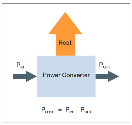
Today's power supply designers and test engineers are generally working to find very small incremental improvements in performance of their device-under-test (DUT). The overall goal is usually to find ways to increase power conversion efficiency, or said another way, reduce losses in the design. Most power conversion loss gets converted to heat, increasing not only the overall power consumption but also affecting other design goals such as battery life, size of heat sinks, and possibly need for cooling fans in some cases - adding cost and potentially reducing reliability. A more efficient design with reduced losses has many benefits.
Sources of loss may be found in nearly every sub-section of a power converter, with key areas of interest often being the switching semiconductors, magnetics, and rectifiers. Performance improvements in the low-digit percent values and fractions of a percent can be meaningful. But to accurately evaluate and measure such small performance increases, the most accurate measurements are critical.
Probe Selection is Step One
When making power measurements, accuracy begins at the probe tip; it is important to choose the right probe for the job.There are several factors that may affect both measurement accuracy and user safety.
Are You Making Ground-referenced or Floating Measurements?
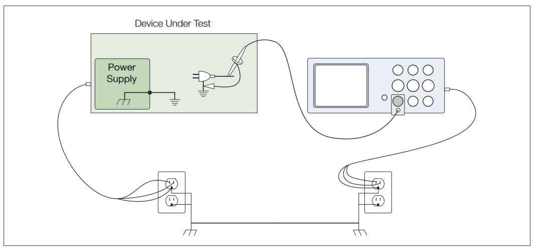
Every voltage measurement is inherently a differential measurement. When the test point to be measured is referenced to equipment ground, things are simplified a bit. Since the oscilloscope chassis is tied to ground, a voltage measurement at such a test point may sometimes be safely made with a single-ended probe, which also references to ground, as shown in Figure 2. In many cases, however, measurements in power converters need to be made on test points where both sides are at elevated potential and groundreference is not possible. In such cases, a differential probe may be not only the clear choice for measurement accuracy but may also be the best choice in the interest of safety.
Voltage Probe Specifications and Selection Criteria
Bandwidth / Rise-time. Choose a probe with sufficient bandwidth, but no more than needed; typically 5x the fastest signal speed. Note: many power supply signals are complex and contain spectral components with frequency values orders of magnitude higher than the fundamental frequency. A good rule of thumb for bandwidth is to pick the fastest edge in your system and use the equation .
Attenuation / Voltage Range. Choose a probe with the minimal attenuation needed to bring the signal into the scope's dynamic range. Each scope's dynamic range can be found on the front panel or in the User Manual. Over-attenuating the signal will push signals down into an oscilloscope's noise floor resulting in inability to see the signal of interest. (More on this to follow.)
Probe Loading. Probe loading can impact measurements and circuit performance, especially at higher frequencies and faster rise times. Low capacitance and high resistance are desirable to minimize effects on the DUT.
Connection Accessories. Having appropriate leads, tips and clips to connect to the DUT is essential to making high-quality measurements and ensuring the integrity of the DUT.
Compatibility with Oscilloscope. Whenever possible, choose a probe that is designed for use with your oscilloscope. Intelligent communication between oscilloscope and probe can enable automatic selection of scaling, units, offset, and termination, along with other benefits.
Important Tips for Improving Voltage Measurement Results
Keep Ground Leads as Short as Possible
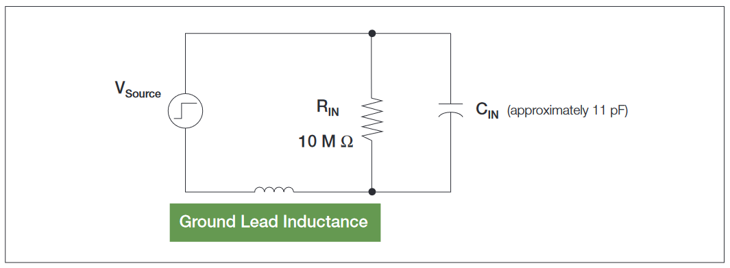
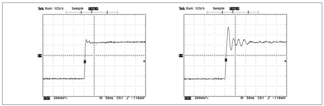
For single-ended probing, it may be tempting to use a long ground lead for convenience when moving the probe tip around to different test points. But a ground lead has distributed inductance, which will interact with the probe's input capacitance to cause ringing at some frequency. This effect is unavoidable, but can be minimized. As the length of the ground lead increases, the inductance also increases and the measured signal will excite ringing at a lower frequency. Figure 3 shows the placement of ground lead inductance in a simplified equivalent circuit and Figure 4 illustrates the effect it has on a rising edge. The ground lead can also act as an antenna, causing magnetic and capacitive noise coupling.
This can be especially problematic when measuring low-level voltages, such as ripple, near switching components or transformers in power converters. To reduce both ringing and noise pickup, use the shortest ground lead possible for critical measurements.
Similarly for differential probes, lead length is also important. The same cautions apply with regard to keeping leads as short as possible, to minimize coupling and noise pickup. When long input leads must be used, a good practice is to twist the two leads together to reduce coupled noise.
Improve Resolution by Removing DC
Measuring a low-voltage AC signal riding on top of a DC signal (ripple or PARD) is one of the most common power converter measurements. To accurately measure the AC signal, one needs to remove the DC portion.
Using AC Coupling
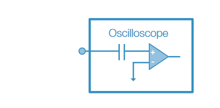
When using a passive probe, one may use the oscilloscope's AC coupling feature to block the DC component at the input and show only the AC signal. AC coupling (or "DC Block") works by inserting a capacitor into the oscilloscope's input path. (See Figure 5.) However, this approach does have some disadvantages, including blocking all DC signal components – even low frequency drift.
Using DC Offset
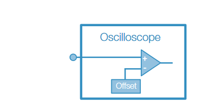
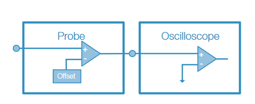
Some oscilloscopes offer built-in DC offset on their internal amplifiers which may be used to eliminate the DC portion of the waveform (Figure 6). Some active probes also offer DC offset on the probe's input amplifier as shown in Figure 7. The TPR4000 power rail probe supports DC offsets of +- 60 V. A few differential probes, such as the TDP1000, feature active offset compensation, as illustrated in Figure 8. Using DC offset is preferable to using AC coupling, since the offset method allows you to see changes in the DC level that may be part of the measured signal. Also by removing the DC voltage component at the beginning of the signal path, the entire dynamic range of the oscilloscope's input is preserved. For differential probes, it may be important to note the Common-mode Rejection Ratio (CMRR) specification of the probe, which represents its ability to reject or ignore any signal common to both inputs, including any DC component.
More on Voltage Rating, Range and Attenuation Factor
To properly match the probe to the measurement task, you need to know the approximate magnitude of the signal to be measured. A general-purpose passive probe might be well-suited to make the measurement, provided the signal does not exceed the voltage rating of the probe. Many passive probes that ship as standard accessories with Tektronix oscilloscopes are rated at 500 VRMS, often with a 10:1 attenuation factor. These probes are a good choice for many general electronics measurements, since they increase the voltage range of the scope and offer relatively high bandwidth. If your test point has a voltage that is <500 VRMS relative to ground, and the signal is in the hundreds of millivolts or higher, you should be able to use such a probe for this basic measurement.

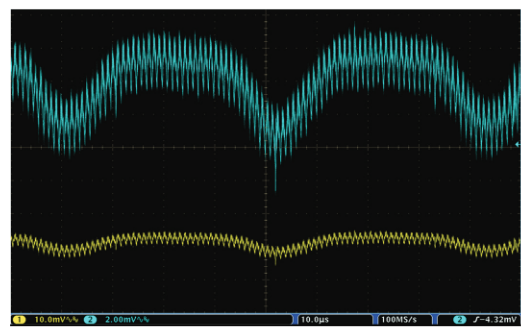
However, for measuring low level signals in the tens of millivolts, a 1:1 (1X) probe may be a better choice, because it does not attenuate the signal as much. Thus, it does not push the signal down into the noise floor of the scope. This benefit in terms of sensitivity is offset by the probe's limited bandwidth, usually around 15 MHz. If this bandwidth is insufficient for your measurement, a passive 2X probe is a better alternative. Consider the case below: measuring AC ripple on a 3.3 V supply.
Ripple Measurement Application
A design engineer was struggling with power supply noise. He needed to probe a 3.3 V supply, but the general-purpose 10X probe he was using didn't provide him with enough sensitivity to see the small ripple voltage, and he couldn't trigger on the periodic noise present in the waveform. Separating noise from ripple voltage can be a significant problem, and this kind of measurement requires a probe with low attenuation. Consider the waveforms in Figure 9. The yellow trace is a 10X probe adjusted to the lowest vertical setting of 10 mV per division and the blue waveform is a 2X probe. The 2X probe can be adjusted down to its lowest vertical setting of 2 mV per division. The output of the power supply produces a signal with 3 mV of ripple, and it is clear why a probe with 10X attenuation is not effective for making this low voltage measurement.
The design engineer understood the benefits of low attenuation probes for making this type of low voltage measurement, and chose the TPP0502 passive probe as well-suited to this task. The engineer made this comment regarding the usability of the 2X probe:
"It was a very simple matter to AC couple the signal and find the 25k Hz ripple that was getting through the front end. Doing the same measurement with an active probe means having to figure out the offset you need and dial it in. Also, thanks to the 300V CAT II rating, I didn't have to worry about accidentally touching one of the adjacent high voltage lines in the power supply. Since it has plenty of bandwidth, I was also able to see some of the other spikes in the power supply that I could be doing a better job of filtering out."
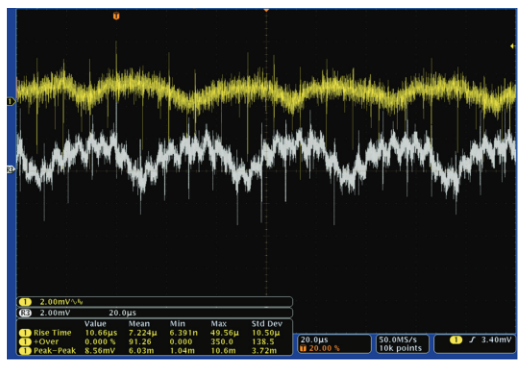
Figure 10 is a plot of the TPP0502 probing a 3.3V power supply node with the scope's vertical sensitivity set to 2mV/ div, the input channel set to AC coupling, and the scope's acquisition mode set to single shot. The white reference trace is the power supply that has the noise leaking into the vertical channel, and the yellow trace is the same signal that is better behaved.
When Do I Need a Differential Probe?
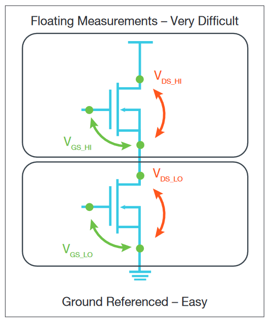
The ripple measurement described above illustrates one application in which a single-ended (ground referenced) probe can be used effectively and safely in power supply design and debug. But many measurements on power-conversion devices need to be made in a floating environment, where reference to earth ground is not available.
Consider these common power-conversion measurements shown in Figure 11:
- Drain to Source Voltage (VDS) on a MOSFET
- Diode voltage on a freewheeling diode
- Inductor and transformer voltages
- Voltage drop across ungrounded resistors
As shown in Figure 11, these components are not tied to ground and differential measurement techniques are required.There are a few different ways to approach differential measurements with an oscilloscope:
- Use two single-ended probes and calculate the difference voltage (Not Recommended!)
- Use an oscilloscope with specially-designed floating inputs.
- Select a differential probe best matched to the measurement (Recommended)
Using Two Single-Ended Probes
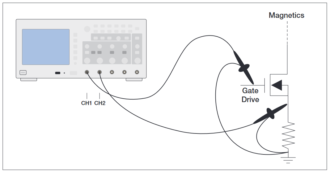
A common technique is to use two single-ended probes with each probe's ground lead tied to earth ground and the tips on either side of the component under test, as shown in Figure 12. The oscilloscope is then set to show the difference between Channel 1 and Channel 2. This is sometimes called “A-B” and it displays the difference voltage between the channels using math in the scope. This technique is sometimes used by engineers when they need to make a differential measurement but don't have the appropriate test equipment available. The measurement setup would resemble Figure 12.
There are several problems with this approach, which all contribute to it being not recommended. This method will provide good measurement results only when the probes and the oscilloscope channels are very well matched (gain, offset, delay, and frequency response). This method also doesn't provide very good common mode rejection (nulling out any AC or DC portion of the signal that is common to both inputs). And, if the two signals are not properly scaled, you run the risk of overdriving the oscilloscope inputs and getting erroneous measurements.
Using an Oscilloscope with Floating Inputs
Using a "floating" oscilloscope, such as the Tektronix TPS2000 or THS3000 Series, is another alternative. Each of the input channels of these oscilloscopes is electrically isolated from chassis ground, and then the oscilloscope is powered by its battery. The parasitic capacitance from the oscilloscope chassis to earth ground is also very low. Together, these isolation characteristics of a floating oscilloscope allow the user to make differential measurements with an insulated passive probe. These instruments are convenient, easy to use, and give good results. However, differential voltage probes offer lower capacitance, are highly balanced, and are available with higher bandwidths.
Using a Differential Probe Matched to the Measurement
For the best measurement accuracy, a differential probe with specifications matched to the measurement task is usually the best choice. Differential probes are active devices. They include a purpose-designed differential amplifier in the probe tip that measures only the voltage across the two test points, regardless of the potential between either test point and ground – greatly simplifying the probing task and eliminating some possible sources of error. And since they measure only the differential voltage, they also have the ability to ignore – and null out – common mode AC swings or DC offset voltages that may be present.
Because measurements in different parts of the device-undertest may have very different requirements, it's important to choose the probe carefully. The guidelines below will help with proper selection.
Differential Probe Application and Selection
Example #1 – MOSFET Switching Device
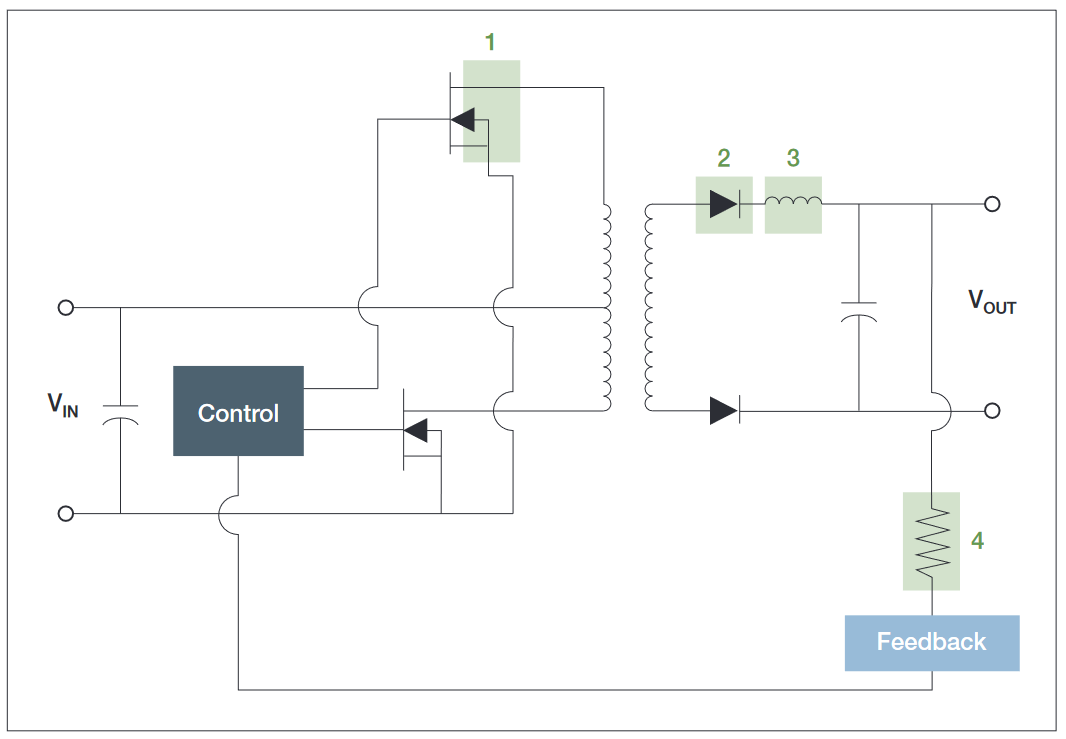
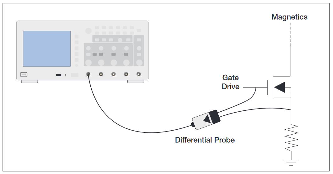
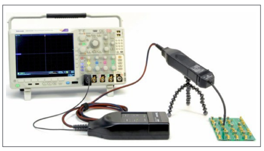
Let's use a common power-supply measurement to illustrate how probe selection can enable the best accuracy and easeof use. In this example, a power supply design engineer needs to measure Turn-on Loss, Turn-off Loss, and Conduction Loss in the MOSFET switching components of the power supply under test. Figure 15 shows a simplified diagram of the circuit's half-bridge topology.
The device under test is a "universal" power supply, designed to be powered from AC line (or "mains") voltage in countries all over the world. This fact alone brings several implications fir the engineer's test requirements – and test equipment:
Measurement Repeatability:
Input voltage ratings for this type of device typically range from 80 VAC to 250 VAC or wider. To characterize performance across a variety of input-voltage conditions worldwide, the engineer will need to perform not just one measurement, but a series of measurements at several input voltage levels. This applies to each performance parameter to be tested. Switching characteristics (and therefore losses) can be expected to be different at each of these input voltage levels, and may not vary in a linear fashion. This increases not only the total number of measurements to be taken, but also the need for repeatability from measurement to measurement.
Voltage Range / Attenuation:
With input supply voltage levels as high as 250VAC, the voltage levels between Drain and Source in the switching MOSFETs can be expected to exceed 500 volts under some conditions. The probing solution needs to be versatile enough to measure these voltage levels along with much lower levels for some tests.
Bandwidth:
In this example, the power supply under test has a switching rate of 25 MHz. Using a common rule of thumb for test & measurement equipment, the probe (and oscilloscope) need a bandwidth at least 5x this speed, or 125 MHz. But this is a simplistic view of real-world signal speeds; the fastest edge in the system determines bandwidth needs, not the switching speed. Spikes, transients and other noise that may need to be investigated will also require higher bandwidths. The same is possible for spikes, transients and other noise that may need to be investigated. If you are measuring signals with rise times in the 10's of nanoseconds, your probe should probably have a rise time spec in the nanoseconds.
The TMDP0200 High-Voltage Differential Probe, for example, has a rise time of less than 1.8 ns. For accurate measurements in this example application, the bandwidth of the measurement system should be on the order of 200 to 500 MHz or higher.
Resistive and Capacitive Loading:
Important specs for voltage probes also include input impedance, a key to possible interaction with the DUT that can compromise measurement accuracy by loading the circuit under test. Two key probe specifications are input R (resistive impedance) and input C (capacitive impedance.) A high input impedance R value (in Ohms) will minimize circuit loading at DC and low frequencies; a low input C value (in pF) will minimize circuit loading at higher frequencies, which can affect timing measurements such as risetime. Tektronix differential probes have input impedance specs that are suitable for most power-electronics applications, but make sure that these probe specs are compatible with the source impedance of your measurement point.
Common-Mode Rejection Ratio:
Common-mode rejection ratio (CMRR) specifies a differential probe's ability to reject any signal that is common to both test points in a differential measurement. In a perfect world, a probe's CMRR would be infinite. However, most differential probes have limitations in this ability, partly because it's impossible to perfectly match the two input leads to each other. CMRR – typically specified in dB - describes the ratio of signal “rejected” by the probe to the amount that leaks through and shows up in the measurement. A key factor in understanding probe CMRR specs is that – for most differential probes – CMRR declines with increasing frequency. Make sure that your probe's CMRR is sufficient to reject common mode signals at your frequencies of interest.
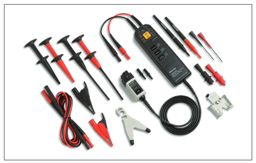
With these requirements in mind, the engineer in this example chose two differential probes to provide the best set of performance tradeoffs for making all the required measurements:
TDP1000 Differential Probe
- +/-100 V voltage rating (DC + pk AC)
- 1 GHz bandwidth
- 5x / 50x attenuation settings
- 1 MOhm input R
- < 1pF input C
- CMRR -50dB @ 1MHz
TMDP0200 High-Voltage Differential Probe
- +/- 750 V voltage rating (@250x)
- 200 MHz bandwidth
- 25x / 250x attenuation settings
- 5 MOhm input R
- < 2pF input C
- CMRR -60dB @ 100kHz; -26dB@100MHz
Example #2 – GaN Switching Device
For some applications, the measurement requirements may exceed the capabilities of even the best conventional voltage probes. In particular, the development of new compound semiconductors based on gallium nitride (GaN) and silicon carbide (SiC) has pushed performance characteristics into territory that offers benefits for the power supply designer, but creates new challenges for measurement.
Let's look at gallium nitride as an example. New switching devices based on GaN may offer smaller chip size, low on-state resistance, and the ability to operate at ultra-high frequencies (> 1MHz) compared to traditional silicon devices. But these desirable performance improvements also create new demands for successful probing and measurement.
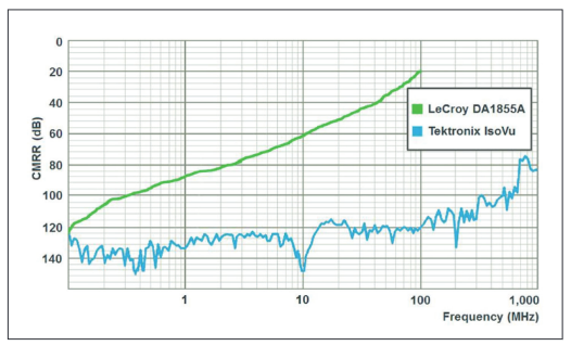
The combination of high voltage and higher switching frequency requires a probing solution with extremely good common-mode rejection (CMRR) at high frequency, especially when making measurements such as gate-source voltage on the high-side semiconductor (refer to Figure 15 on p.11.) But even the best conventional differential probes lose CMRR performance as frequency increases. An entirely new approach to probe design is needed to overcome this inherent limitation.
Tektronix has developed a revolutionary new design, called IsoVu, which addresses this emerging need. Unlike all other commercially available probes, IsoVu has no electrical connection to the scope. It uses lasers for the analog signal path, power over fiber, feedback and control. Because it is built using optical technology, IsoVu electrically isolates the device-under-test from the the oscilloscope. This allows an incredible Common Mode voltage rating, unbeatable CMRR over the entire bandwidth, and significantly higher bandwidth than traditional high voltage differential probes. Refer to Figure 18 below. The new probes also offer up to 1GHz bandwidth and common-mode voltage rating up to 2000 Vpk, along with low input C. These characteristics make IsoVu an indispensable and unique tool for making measurements on the latest power semiconductor technologies.
IsoVu Differential Probes
- Up to 60kV common mode voltage rating
- Up to +/- 2500 V differential voltage rating
- Up to 1 GHz bandwidth
- 10 M[omega] input R
- 3pF input capacitance
- CMRR -110dB @ 100 MHz, -91dB @ 500 MHz
Beyond Probing – the Measurement System
Selecting and properly using the best probe for your application is an important first step, but integrating the probe into the rest of the measurement system is equally important to assure measurement accuracy and repeatability through the entire system. Probes like the TDP1000 and TMDP0200 connect to oscilloscopes using the TekVPI® interface, designed to work as a seamless system with Tektronix oscilloscopes in the MSO/DPO2000, MDO3000, MDO/MSO/DPO4000 and MSO/DPO5000 Series, as well as 3/4/5/6 Series oscilloscopes. This interface not only provides power to the active probes, but also communicates intelligently to automate probe functions such as attenuation settings, AutoZero, DC offset, Autorange, and more.
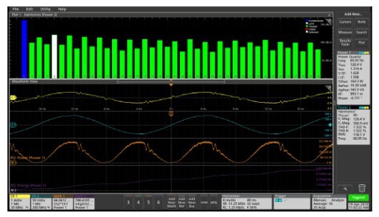
Automated Power Measurement Application
The third piece in the "total system" approach is applicationspecific automation software to run on the oscilloscope. Software applications such as DPOPWR and 3/4/5/6- PWR dramatically speed up cumbersome calculations by automating measurements such as switching loss, power factor, magnetic analysis, control loop response, and more.