Introduction
With decreased MOSFET gate length, hot carrier induced degradation has become one of the most important reliability concerns. In the hot carrier effect, carriers are accelerated by the channel electric fields and become trapped in the oxide. These trapped charges cause time dependent shifts in measured device parameters, such as the threshold voltage (VTH), transconductance (GM), and linear (IDLIN) and saturation (IDSAT) drain current. In time, substantial device parameter degradation can occur, resulting in device failure. Instrumentation for measuring HCI must provide these three key capabilities:
- To extract device parameters automatically.
- To create a stress-measure sequence with a variety of stress times.
- To export the measure data easily for advanced analysis.
This application note describes how to use these key capabilities in the Keithley Model 4200-SCS (Semiconductor Characterization System) to perform hot carrier degradation testing
The MOSFET Hot Carrier Effect
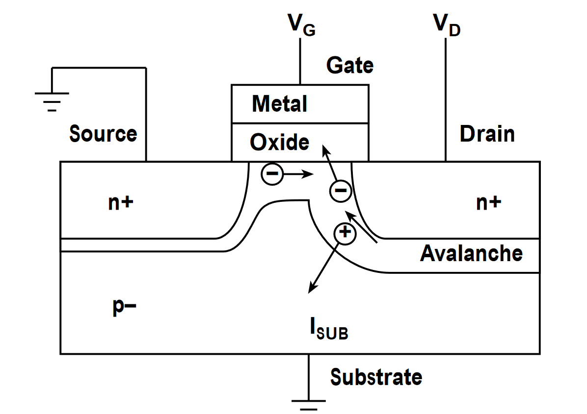
Today’s ULSI MOSFET devices feature extremely short channel lengths and high electric fields. In these high electric fields, carriers are accelerated to high velocities, reaching a maximum kinetic energy (hot) near the device drain. If the carrier energy is high enough, impact ionization can occur (Drain Avalanche Hot Carrier Effect), creating electron-hole pairs (Figure 1). These holes and electrons can attain enough energy to surmount the Si–SiO2 barrier and become trapped in the gate oxide. Trapped charges cause device degradation and enhanced substrate current (ISUB).
Monitoring Hot Carrier Device Performance
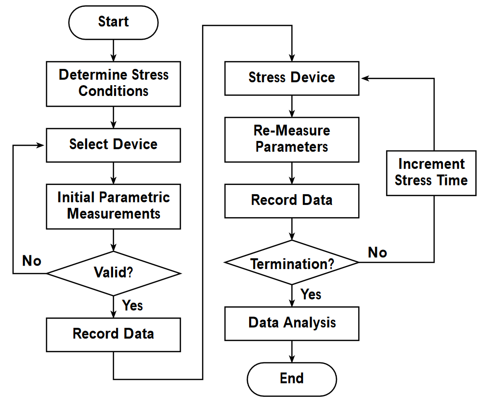
Figure 2 illustrates the hot carrier test methodology. Hot carrier device test times are typically very long, so the first step is to determine an optimized set of stress conditions. Then, a new device is selected and initial device parameters such as VTH, GM, I DLIN and IDSAT are determined. The optimized stress is then applied for a specified stress interval. After each stress interval, parametric measurements are made again and the degradation determined. This test-stress cycle continues until the target degradation or test time criteria are met. The hot carrier lifetime is determined from the degradation vs. stress time data.
Hot Carrier Lifetime Using the Keithley 4200
Determining Stress Conditions
Before hot carrier testing begins, the drain and gate stress bias voltage must be established. To ensure realistic channel hot carrier conditions, the recommended maximum drain stress bias voltage is less than 90% of the device’s drain-to-source breakdown voltage.
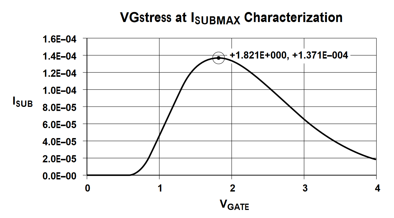
At a given drain stress bias voltage, the gate stress bias (VGstress) should be selected to maximize hot carrier degradation. For NMOS devices, this typically occurs at a gate bias (VGATE) that maximizes the substrate or bulk current (ISUB). Figure 3 represents typical 4200-SCS ISUB vs. VGATE data. In this case, the optimal VGstress is 1.821V.
Determining Device Parameters
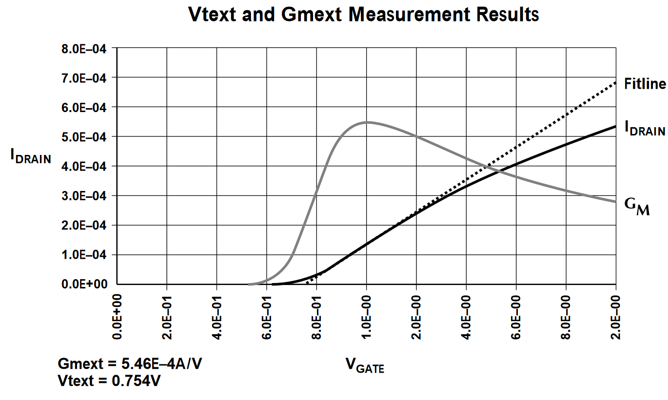
Hot carrier monitored parameters include VTH, GM, IDLIN and saturated I DSAT. These parameters are initially determined before stress and redetermined at each cumulative stress time. The IDLIN is the measured drain current with the device biased in the linear region, while IDSAT is the measured drain current with the device biased in the saturation region. VTH and GM can be determined using either constant current or extrapolation methods. In the extrapolation method, the VTH is determined from the maximum slope of the IDS vs. VGS curve.
The 4200-SCS’s Formulator Tool greatly simplifies extracting these parameters. The built-in functions include Differentiate to obtain GM, a MAX function to obtain the maximum GM (Gmext), and a least squares line-fit function to extract VTH (Vtext). Figure 4 illustrates the Formulator’s automated data analysis capability
Stressing the Device
After measuring the device parameters, the device is stressed at the drain and gate stress bias conditions for a specified time. Cumulative stress times are typically logarithmic, e.g., 10, 30, 100, 300, 1000, etc. At each cumulative stress time, the device parameters are measured again and recorded.
The 4200-SCS’s built-in test sequencer and Interactive Test Module (ITM) capability greatly simplify implementing the hot carrier test procedure. Figure 5 depicts the hot carrier stress test sequence in the Project Navigator window and the hot carrier stress test module (hcistress10) DefinitionTab. The Project Navigator window displays the test sequence, which begins by making initial measurements of the idlin, idsat and vtlin (the vtlin module extracts parameters Vtext and Gmext). The hcistress10 test then applies a ten-second stress at the specified drain and gate stress voltages. Once the stress is complete, device parameters are measured again. This stress-measure sequence continues until the maximum specified stress time is exceeded.
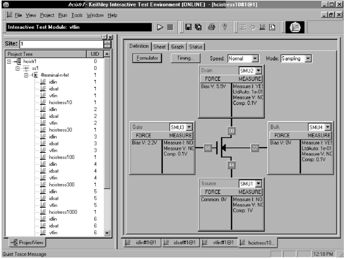
The hcistress10 test Definition Tab is used to specify the stress voltages and stress times. In this example, the gate and drain stress conditions are specified as 2.2V and 5.5V, respectively. The stress time is specified in the Timing dialog box (not shown), which is activated using the Timing … Command Button (see Figure 5). In the Timing dialog box, the hcistress10 test is set to Sampling Mode with an interval of one second and ten samples. This will provide a ten-second stress. To obtain longer stress times, simply increase the number of samples or the sampling interval.
Data Analysis
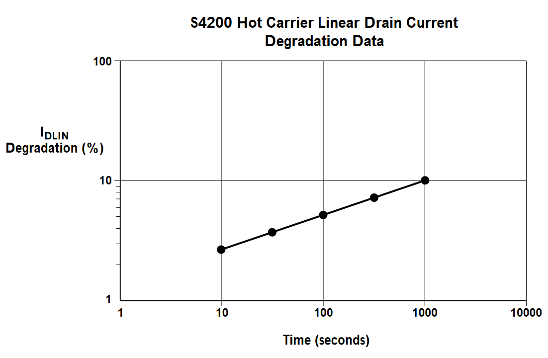
N-channel hot carrier degradation vs. time data typically exhibit linear behavior when plotted on log-log plots. Least-squares fit regression analysis is used to interpolate or extrapolate the hot carrier time to target lifetime. Target device lifetime is defined as a 10% parameter change or, in the case of VTH, a change of 50mV from its unstressed value.
The 4200-SCS automatically saves raw sweep data and extracted test results to fully compatible Microsoft Excel® spreadsheets (data file extension: .XLS), which greatly simplifies hot carrier data analysis. Figure 6 shows 4200-SCS IDLIN degradation data vs. stress time. In this case, the projected time to target failure is 1004.7 seconds.
Conclusion
The 4200-SCS greatly simplifies the determination of hot carrier induced degradation. Built-in 4200-SCS software tools, such as the Project Navigator, Formulator, and a fully compatible Excel data format, provide a flexible, fast, and easy-to-use test environment. Furthermore, the 4200-SCS links these tools with advanced Source-Measure Unit technology to create an ideal test environment for challenging device reliability and characterization requirements.