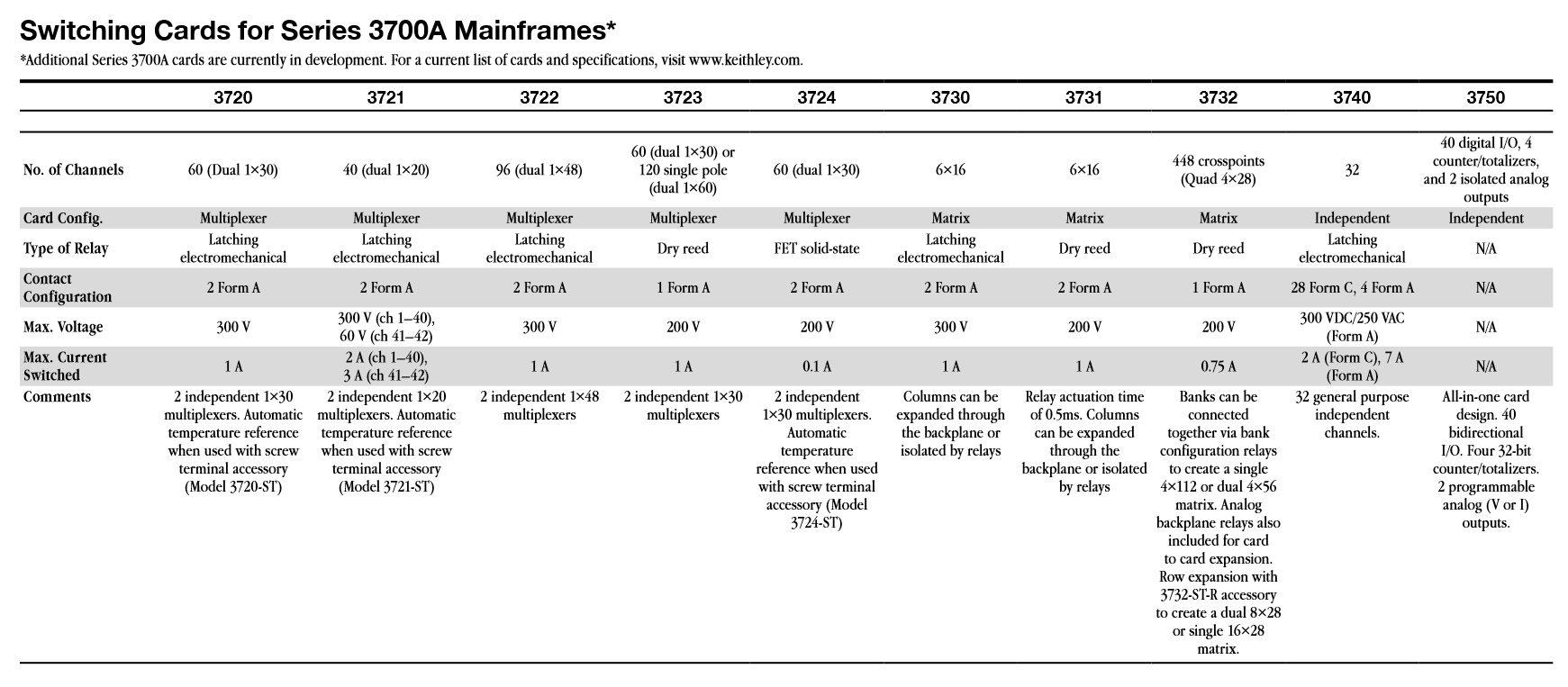
Introduction
Many electronic test systems use relay switching to connect multiple devices to sources and measurement instruments. In some cases,multiple sources and measuring instruments are connected to a single device. Switching allows automating the testing of multiple devices,thereby reducing error and costs.
Designing the switching for an automated test system demands an understanding of the signals to be switched and the tests to be performed. Test requirements can change frequently, so automated test systems must provide the flexibility needed to handle a variety of signals. Even simple test systems often have diverse and conflicting switching requirements. Given the versatility that test systems must offer, designing the switching function may be one of the most complex and challenging parts of the overall system design.
As a signal travels from its source to its destination, it may encounter various forms of interference or sources of error. Each time the signal passes through a connecting cable or switch point, the signal may be degraded. When calculating the overall system accuracy, the engineer must include not only the effects of the switch itself but all the switching hardware in the system.
The quality of a switch system depends in large part on its ability to preserve the characteristics of the test signals routed through it. For example, when the test signal is a low voltage, the switching system must minimize errors such as offset voltage and IR drops. Leakage current may be a problem for high resistance and low current switching applications. Depending on the type of test signal involved, specific switching techniques must be used to maintain signal integrity through the switch system. This e-handbook describes switching techniques for a variety of test signals.
Voltage Switching
Many different applications involve switching a voltmeter or voltage source to multiple devices, including testing batteries, electrochemical cells, circuit assemblies, thermocouples, etc.
The types of switch cards and the techniques used in these applications will depend on the magnitude and impedance of the voltages switched.The approximate level for low voltage switching is in the millivolt range or less, mid-range levels are from 1V to 200V, and voltages greater than 200V demand the use of high voltage switching methods.
Switching a Voltmeter to Multiple Sources in Series
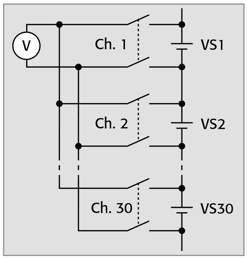
Figure 1 illustrates switching a voltmeter to a series string of 30 batteries or voltage sources (VS). To avoid short-circuiting one or more of these sources, it is necessary to open a given channel before closing a second one (breakbefore-make operation). To guard against short-circuiting,add fuses in series with each voltage source to prevent damage to the switch card. Be sure not to exceed the commonmode rating of the switch card.In this example, each battery is 12V and the total voltage across the string is 360V. A channelto-channel voltage rating and a common-mode voltage rating of at least 500V is desirable.
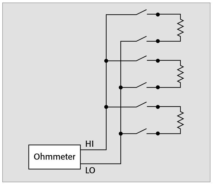
Switching a Voltage Source to Multiple Loads
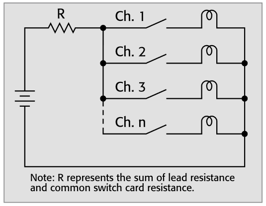
Figure 2 shows a single voltage source connected to multiple loads, such as lamps. If two or more loads are connected to the source, the voltage at each load may be less than expected due to current flow through the common impedances (R), such as the test leads and trace resistance.As additional loads are connected, the total current will increase, thereby increasing the voltage drop across the common impedances (R).
Switch Resistance
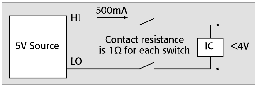
When switching a voltage source to multiple devices, it may become necessary to compensate for voltage drops due to switch resistance. In particular,if the devices have low resistance, the current flowing through the switches may cause a significant voltage drop.To prevent this problem, remote sensing can be used to correct for any voltage drops in switches and wiring. With remote sensing, external sense connections are made across the load. Therefore, the subsequent programmed output voltage will be the actual voltage across the load.
For example, Figure 3a shows a 5V source being switched to an integrated circuit (IC). The contact resistance for each switch is 1Ω. If the current drawn from the source is 500mA, the voltage drop across each switch will be 500mV, and the voltage at the integrated circuit will be reduced by a total of 1V. Operation of the IC will likely be unsatisfactory. Figure 3b shows a 5V source with remote sense. In this case, sense leads are also connected to the load. This will ensure that the actual voltage across the load will be 5V, and the IC will operate as intended. Note that the voltage at the source output terminals is 6V.
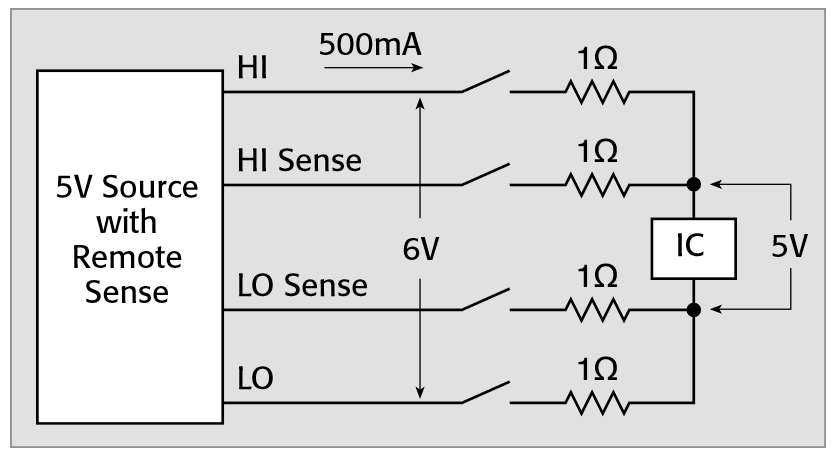
Do not use hot-switching with remote sensing since the voltage from the source may become excessive during switching.
Low Voltage Switching
When switching low voltage signals (millivolts or less), special techniques must be used to avoid unwanted voltage errors. However, the required accuracy will determine if these techniques are necessary. These unwanted voltage errors may be due to thermoelectric offset voltage in the switch card and connecting cabling, switch film contamination, magnetic interference, and ground loops. For more information on low voltage measurements, refer to Keithley's Low Level Measurements Handbook.
Thermoelectric Offset Voltage
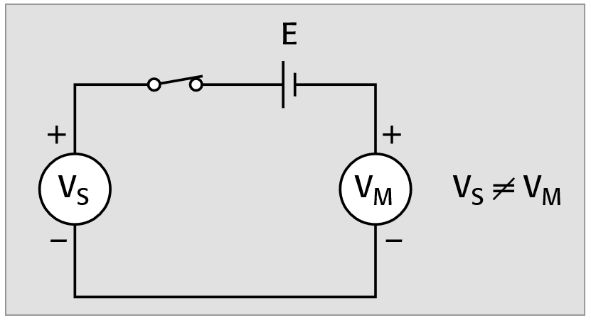
The contact potential or thermoelectric offset voltage is the key specification of a switch card designed for low voltage switching.Thermoelectric voltage is the voltage generated by thermal differences at the junction of dissimilar metals, such as between the nickel-iron reed relays and the copper conductor to which they are connected.The temperature gradient is typically caused by the power dissipated by the energized coil. The offset voltage adds directly to the signal voltage and can be modeled as an unwanted voltage source in series with the intended signal. The offset voltage will cause an error in the applied stimulus to a device under test or the value measured by the voltmeter.
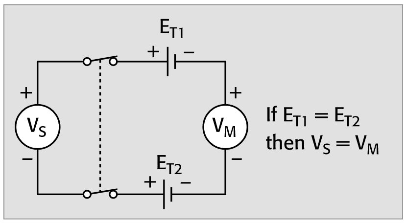
As shown in Figure 4a, the offset voltage (E) of a single pole relay is added into the circuit. As a result, the measured voltage (VM) will be the sum of the source voltage (Vs) and the offset voltage (E). To minimize this offset voltage, a low voltage switch card uses a two-pole relay, as shown in Figure 4b. Here, the offset voltage (ET1) in the circuit HI is largely canceled by the offset voltage (ET2) in circuit LO. The contact potential of some low voltage cards is specified with the card used as a two-pole switch to take advantage of this cancellation. It may be specified as "per contact pair." However, total cancellation cannot be achieved because temperature differences will cause ET1 and ET2 to be slightly different.
The drift due to the thermoelectric voltage of a switch card depends on several factors, including the type of relays used (reed, solid-state, or electromechanical). The drift also depends on the coil drive technique (latching or non-latching). Finally, the material used for the contact plating (for example, nickel alloy or gold) also affects the thermoelectric voltage.
The power dissipated in the coil of the reed relay may cause the temperature to increase for several minutes after it is energized, so it is important to make low voltage measurements within a few seconds after contact closure. If many measurements are taken over several minutes after closure, a steadily increasing thermoelectric voltage will be added to the reading. Thermal time constants may range from seconds to hours. Even though solid-state relays have no coil dissipation, heat generated by internal IR drops can still produce thermoelectric drift.Latching relays use a pulse of current to actuate them, so they have very low thermoelectric drift.
The connections to the switch card itself represent another source of thermally generated voltages. Wherever possible, make connections to the card with untinned copper wire, and keep all leads at the same temperature.
The thermoelectric offset voltage due to the switch card and the interconnecting cable may be compensated for by using a short-circuited channel to establish a zero reference. Connect a clean copper wire connected between the HI and LO terminals of an unused channel. Close the channel and measure the offset voltage. Then open this channel.This value can be subtracted from subsequent readings made on other channels. This approach is not ideal because the offset will change over time due to self-heating and changes in the ambient temperature.
When switching low voltages while making low resistance measurements, the thermoelectric offset voltages may be canceled by using offset compensation. This technique requires making two voltage measurements with two different values of current. To determine the resistance, the difference between the two resulting voltages is divided by the difference of the two test currents:
| R = | V1-V2 |
| I1- I2 |
Refer to the section on "Low Resistance Switching" for more information on this method.
Switch Film Contamination
Over time, a contaminating film can form on the surface of a relay contact. This film can increase the relay contact resistance, which can make the switched voltages erratic when measuring or sourcing low voltage. Voltages greater than 100mV are usually sufficient to clear this contamination. Using scanner cards with solid state switches is one way to avoid this problem.
Magnetic Interference
Magnetic interference can be a problem in low voltage circuits. A high rate of change in magnetic flux, such as that produced by a switching power supply or by switching a high current signal on and off, can induce a pulse of many microvolts in an adjacent circuit. This can easily cause significant error in a low voltage circuit. This type of interference can be minimized by separating the noise source and the sensitive circuit as much as possible,by magnetic shielding, and by reducing the enclosed area of the noise source and signal conductors. Twist the HI and LO wires of each channel together to minimize the enclosed area.
Ground Loops
Ground loops can easily occur in a complex test system. If a small potential difference exists between two ground points, some ground currents may flow through a sensitive part of the system. This may occur only when certain switches are closed, so it can be very difficult to diagnose. When possible, try to maintain a single system ground point.When this is not possible, isolation techniques using optical coupling or balanced transformers may help by increasing the effective resistance between the two points, thereby reducing the common ground current to a negligible level.
High Voltage Switching
Some applications, such as testing insulation resistance of cables and printed circuit boards and high-pot testing, may require switching high voltages. To avoid switch card damage, be particularly careful when switching voltages of ~200V or higher.
Choose a card rated for the desired voltage and power levels. Cold switching, if feasible, will extend the relay life and make it possible to increase the allowable current. Be sure to use appropriately rated cables when switching high voltages.
Reactive loads can cause excessive current and voltage transients,so current surge limiting for capacitive loads and voltage clamping for inductive loads are required to prevent damage to the relays and external circuitry.
The surge current from a capacitive load is i = C dV/dt and must be limited to less than the rated current to protect the relays. Figure 5 shows a series resistance (R) used to limit the charging current. The resistor must be able to withstand the applied voltage; otherwise, the high voltage may arc across the resistor, damaging the device under test and the switch card. All components must be rated for peak voltage and current.
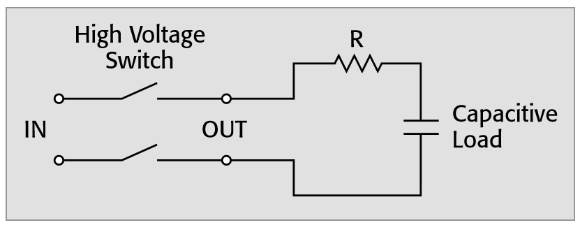
When determining the current limit for a reactive load, consider the maximum load in VA. For example, if the maximum load is 10VA and 500V is switched, then the current must be limited to 20mA. The series resistance is then calculated as:
| R = | 500V | 25kΩ |
| 20mA |
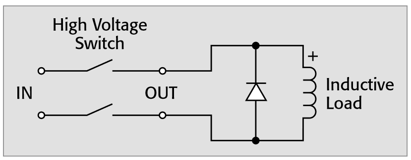
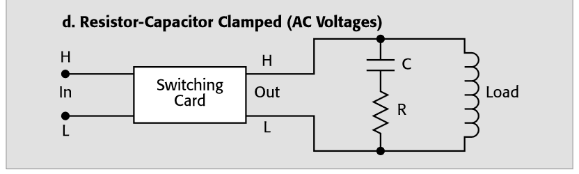
Inductive reaction voltage (L(di/dt)) must be less than the scanner card's maximum voltage rating. Figure 6 shows two typical clamping circuits,one using a diode for clamping DC voltages and the other using back-toback zener diodes for clamping AC voltages.
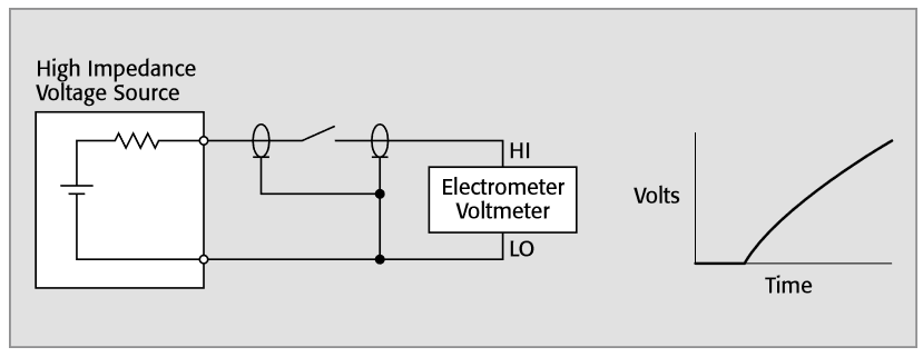
High Impedance Voltage Switching
High impedance voltage switching may be necessary in applications such as monitoring electrochemical cells and measuring semiconductor resistivity. Switching and measuring voltage sources with high internal impedance are subject to a number of errors, including offset currents,stray leakage paths, and electrostatic interference. Shunt capacitance may increase the settling time. This section discusses these error sources and provides an example application.
When choosing a card to switch high impedance voltage, make sure the card has a low offset current. Any offset current flowing through a high impedance device will cause an unwanted voltage to appear across the device. This offset voltage will be added to the voltage measurement.High impedance circuitry is susceptible to electrostatic interference, so use shielding to avoid noise pickup. The device under test, as well as the connecting cables, should be well shielded.
Leakage paths can cause error by reducing the measured voltage. Such leakage paths may be present in the test instrument, switching cards,cables, and fixtures. To minimize errors due to such leakage paths,choose a switch card with high isolation resistance and use guarding wherever possible, including in the test fixturing and cabling. Also, select insulating materials with the highest possible insulation resistance.
Response time is another concern when switching high impedance voltage signals. Excessive response time may be caused by shunt capacitance, both in the switch itself and in the associated cables. In some cases, the shunt capacitance can be largely neutralized by the use of a driven guard, which will keep the shield of the cable at nearly the same potential as the center conductor (or high impedance lead) of the cable. Figure 7a shows a high impedance voltage connected through a switch to an electrometer voltmeter. Notice the slow response to a step function. To guard the signal, make a connection between the guard output (unity gain or preamp output) of the electrometer and the shield of the switch card, as shown in Figure 7b. Some electrometers, such as Keithley's Model 6517B and Model 6514, can make this connection internally by enabling the internal guard connection. Enabling the guard effectively reduces the cable and switch capacitance, thereby improving the electrometer's response time.
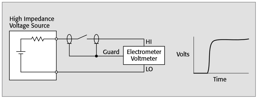
Switch cards appropriate for high impedance voltage switching include the Models 7158 and 6522. A card with triax connections is necessary if the guard voltage could exceed 30VDC. This precaution is necessary to ensure safety.
Current Switching
Applications for current switching include testing of power supplies,insulation resistance, capacitor leakage, resistivity of materials, batteries,and semiconductors. This section discusses current switching in general.Special techniques are required when switching high current or low current. Current switching applications may require connecting multiple current signals to a single meter, or may require connecting a single source to multiple loads.Each case has different switch configurations and concerns.
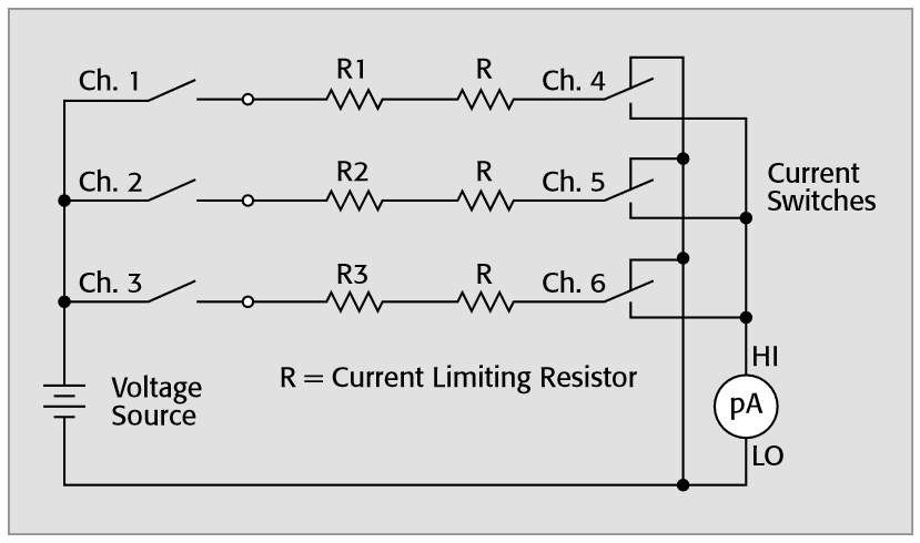
Connecting Multiple Current Signals to a Single Ammeter
Most current measuring applications require that all current paths be continuous, even when a particular current signal is not connected to the ammeter. To accomplish this, switch cards designed for current switching often use SPDT or Form C relays. As shown in Figure 8, when a channel is in an open state (i.e., not connected to the output),signal HI is connected to signal LO through the normally closed (NC) contact. In this case, only signal HI is switched. Signal LO is hardwired to the ammeter and to all other signal LOs. This is normally the case when testing components with relatively low currents (<1μA). When a channel is selected, the current source is connected to the ammeter through the normally open (NO) contact. Note that the current will be interrupted briefly when the Form C relay is actuated. This could cause problems when used with high speed logic or other circuits sensitive to a momentary break in the current flow. This problem can be overcome by using a switch card with a pair of Form A isolated switches to provide a make-before-break (make/break) connection.
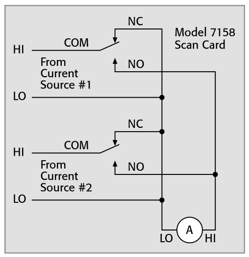
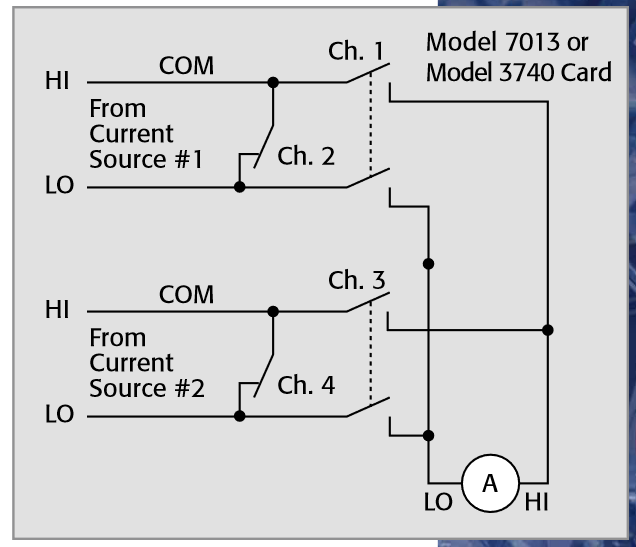
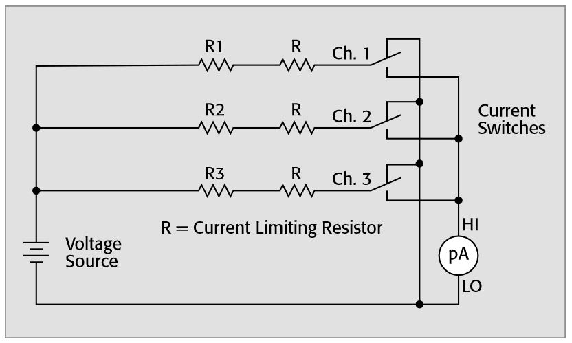
Figure 9 illustrates using a switch card with isolated Form A relays to maintain the current path. In this example, one relay (Ch. 1) is used to connect Current Source #1 to the ammeter. A second relay (Ch. 2) is kept in the closed position to provide a path when the current is not being measured. If using a card such as the Model 7013 Relay Switch Card in a Series 7000 mainframe or the Model 3740 Isolated Switch Card in the Model 3706A mainframe, Ch. 2 is normally energized. This relay is opened when the measurement is made, but not until after Ch. 1 is closed. This circuit is used when switching moderate-level current (milliamps to amps range) when the current cannot be interrupted even for a moment. Note that with this circuit, the LO terminals of the current sources are isolated from each other, unlike the circuit in Figure 8.
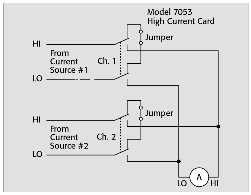
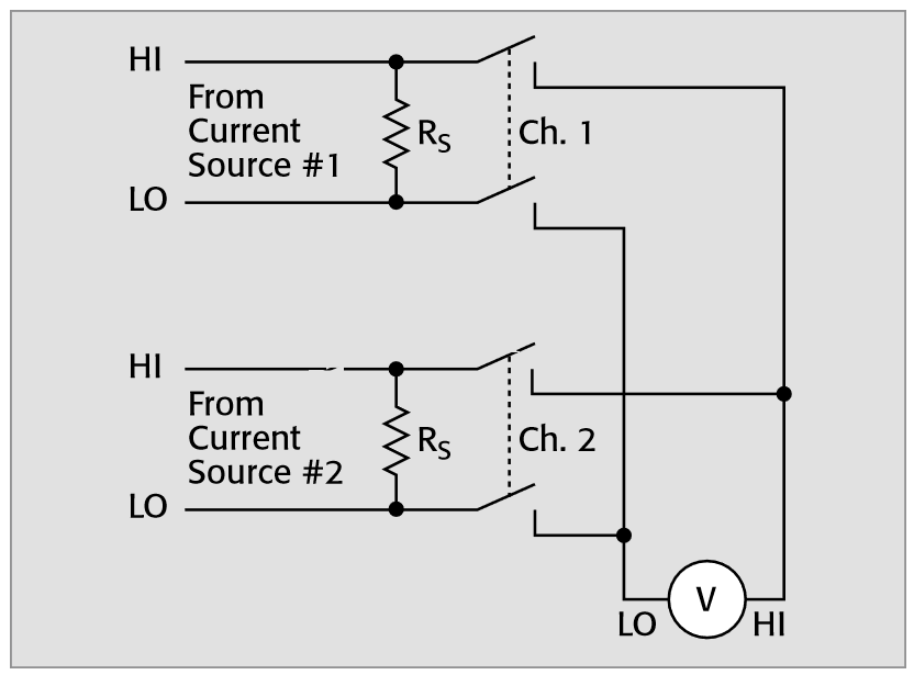
The Model 7053 High Current Card is another card that is often used to switch current. As shown in Figure 10, this card uses a dual Form C relay. The jumper ensures a continuous path, but it can be removed when using the card to switch voltage. Because this is a Form C relay,the current will be momentarily interrupted when the relay is energized or de-energized. An alternative to switching the current loop is to place a shunt resistor in the loop. The voltage drop across the resistor (RS) is then measured as shown in Figure 11. The voltage readings are then converted to current using Ohm’s Law. This technique can be used when the range of current is relatively narrow, such as approximately two decades. The resistor (Rs) should be no greater than the ratio of the maximum allowable voltage drop to the maximum current. Choose a value with a convenient scale factor, such as 1, 10, or 1000Ω, so that it will be easy to calculate the current. Once the value of the resistor is chosen, verify that the minimum voltage drop will not be so small that it will be difficult to measure with the voltmeter.
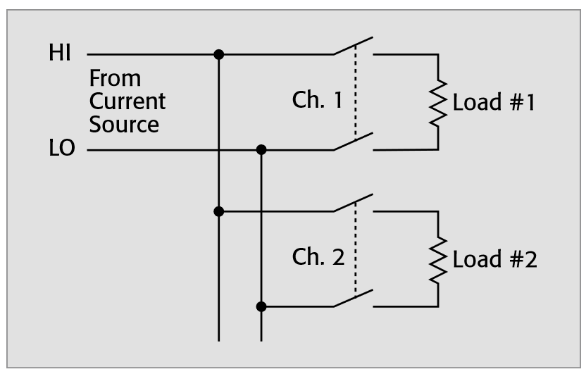
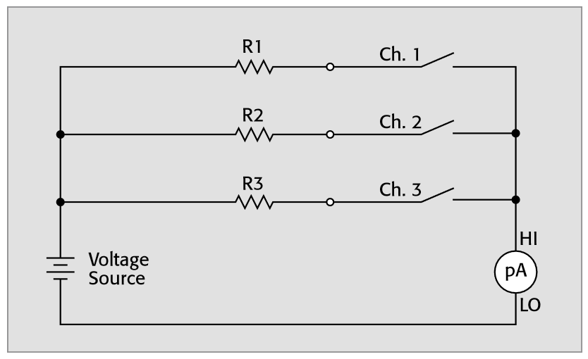
Connecting a Current Source to Multiple Loads Unlike switching current signals to an ammeter, switching a current source to multiple loads usually does not require maintaining the current path at all times.
For this case, a card with Form A switches is suitable, as shown in Figure 12. To connect the current source to Load #1, close relay Ch. 1. Ensure that Ch. 1 is opened before Ch. 2 is closed if the loads are capable of storing energy, such as a battery or a large capacitor. Two high energy loads connected in parallel may damage the relays.
Often, cards designed for voltage switching can be used for current switching for currents from 1A to 1μA. For current less than 1μA, choose a card that has high isolation resistance (across open contacts, from high to low, and between channels) and low offset current.
Cold switching is always preferable to ensure maximum relay life. Cold switching involves turning the source current off (placing it on standby) before opening or closing a relay.
High Current Switching
When designing a switching circuit for high current (>1A), pay particular attention to the maximum current, maximum voltage, and VA specifications of the switch card. Also, it's important to choose a switch card with low contact resistance to avoid excessive heating that can cause contact failure by welding the contacts together. Contact heating is caused by I2R power dissipation.
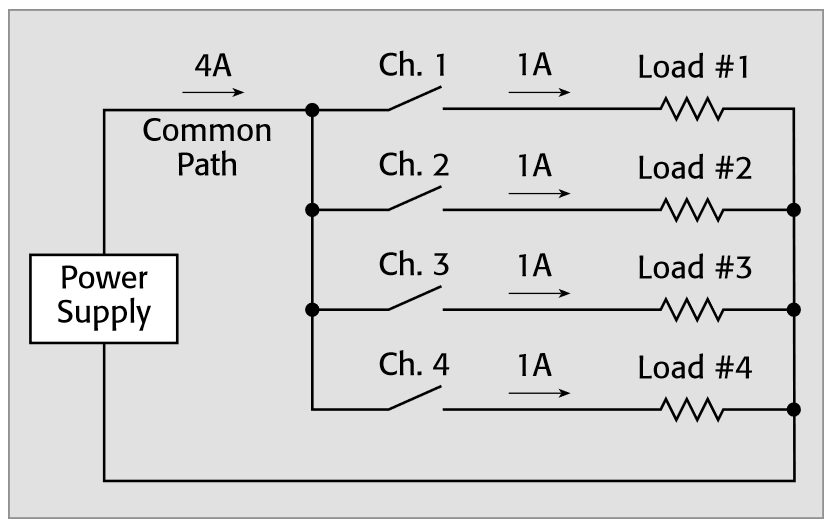
High current switching can be used for either switching a power supply to multiple loads or for switching an ammeter to multiple sources. Figure 13 is an example of switching a power supply to multiple loads using a multiplexer scanner card. In this example, the power supply will output 1A to each of four loads. This doesn't present a problem when only one channel is closed at a time. However, when all four channels are closed,the power supply will output 4A through the common path. Unfortunately,even though the maximum current of a particular channel is specified at 1A, the common path on the switch card may not be able to tolerate 4A.This is not usually specified for a switch card, but the limitation is usually a function of the trace width and connector ratings. One way to avoid this problem is to use a switch card with independent (isolated) relays and connect with wires rated to carry the total current.
When currents that exceed the commercially available card ratings must be switched, then a general-purpose switch card can be used to control external high current relays or contactors. The user must supply the coil current for the external relays.
Under no circumstances should unlimited power (direct from the power line) ever be connected directly to a switch card.
When switching high VA loads (power line to motors, pumps, etc.), solidstate relays (SSR) are often used. Industry standard SSR modules are available from many sources. These SSR modules are plugged into a board, such as the Keithley Model PB-24SM, that can be controlled from TTL-level digital outputs. These digital outputs can be from a board that plugs into a PC or from a scanner mainframe. Some SSR modules can switch up to 1kVA to high power loads.
Concerns about switching transients with reactive loads also apply to high current switching. Cold switching, where contacts do not make or break current or voltage, is recommended for currents in excess of 100mA to avoid radiated interference and to extend relay life.
Table 1. High Current Switches
| Card Model | Current Rating | Compatible Mainframes |
| 7053 | 5A (10 channels) | 7001, 7002 |
| 7700 | 3A (two channels) | 2700, 2701, 2750 |
| 7702 | 3A (two channels) | 2700, 2701, 2750 |
| 7705 | 2A (40 SPST Isolated) | 2700, 2701, 2750 |
| 3740 | 3A (28 SPST Isolated) 7A (4 SPST Isolated) |
3706A |
| 3721 | 2A switched, 3A carry (40 channels) 3A (2 channels) |
3706A |
| 3730 | 6×16 Matrix (1A switched, 2A carry) | 3706A |
| 7174A | 2A carry | 707A/708A |
Low Current Switching
When switching currents of 1μA or less, special techniques must be used to minimize interferences, such as offset currents, leakage currents,electrostatic interference, triboelectric currents, and electrochemical currents. These types of interferences may be due to the scanner card itself, the connecting cables, or the test fixturing. Allowing sufficient settling time before making a measurement is also crucial when switching low current.
Offset Currents
The offset current specification of the switch card should be as low as possible for switching low current. Offset current is a spurious current generated by a switching card even though no signals are applied.It is usually caused by galvanic sources on the card. Offset current is especially significant when measuring low currents if the magnitude of the offset is comparable to the low current being measured. Scanner cards designed to minimize offset current are commercially available. For example, the Model 7158 Low Current Scanner Card has <1pA offset current (typically <30fA).
To measure the offset of a switch card, connect the output of the card to a picoammeter or electrometer. Make sure all input connections on the scanner card are shielded. If the card has triax or BNC connections,cap each input channel. Close each channel individually and measure the offset current after allowing the switching transients to decay and the current to stabilize. If the offset currents for the different channels are reasonably stable, a correction factor can be stored in the control computer to allow more accurate low current measurements. This is done by subtracting the offset current for a given channel from subsequent measurements made via that channel.
Leakage Currents
Leakage current is an error current that flows through insulators when a voltage is applied. It can be found on the switch card, in the connecting cables, and in the test fixture. Even high resistance paths between low current conductors and nearby voltage sources can generate significant leakage currents. Use a card with high isolation, guard the associated test fixtures and cables, select proper insulating materials, and clean the circuit boards to reduce these effects.
To minimize extraneous current paths (or leakage current), use a switch card that has high channel isolation resistance (the isolation between channels). When switching a current to be measured, high input isolation (the isolation between input HI and LO), is not as critical as channel isolation because there is normally very little voltage present, only the voltage burden of the ammeter. However, when switching a current source, very high voltage can be present across the input depending on the load resistance; therefore, high input isolation becomes critical.
To determine the leakage current at a particular voltage, apply a step voltage of this magnitude to the circuit. This generates a transient current that will gradually decay to a steady value, which is the leakage current of the system for that particular path. Once the leakage current is determined, it can be subtracted from subsequent readings on a particular channel. However, the leakage current is dependent on the applied voltage, so this technique cannot be used for voltage sweeps.
To prevent leakage current on the switch card, take special care when handling to prevent degradation of performance. Handle the switch card by the edges to avoid contaminating it with dirt, body oil, etc. If cleaning the board becomes necessary, follow the instructions in the manual provided with the switch card. Humidity can also increase leakage current. Placing the switch system in a low humidity room will minimize this effect. Switch cards are typically specified to operate in relative humidity of 50% or less
One way to reduce leakage currents in the test fixturing is to use good quality insulators such as Teflon® and polyethylene. Avoid materials such as nylon and phenolics.
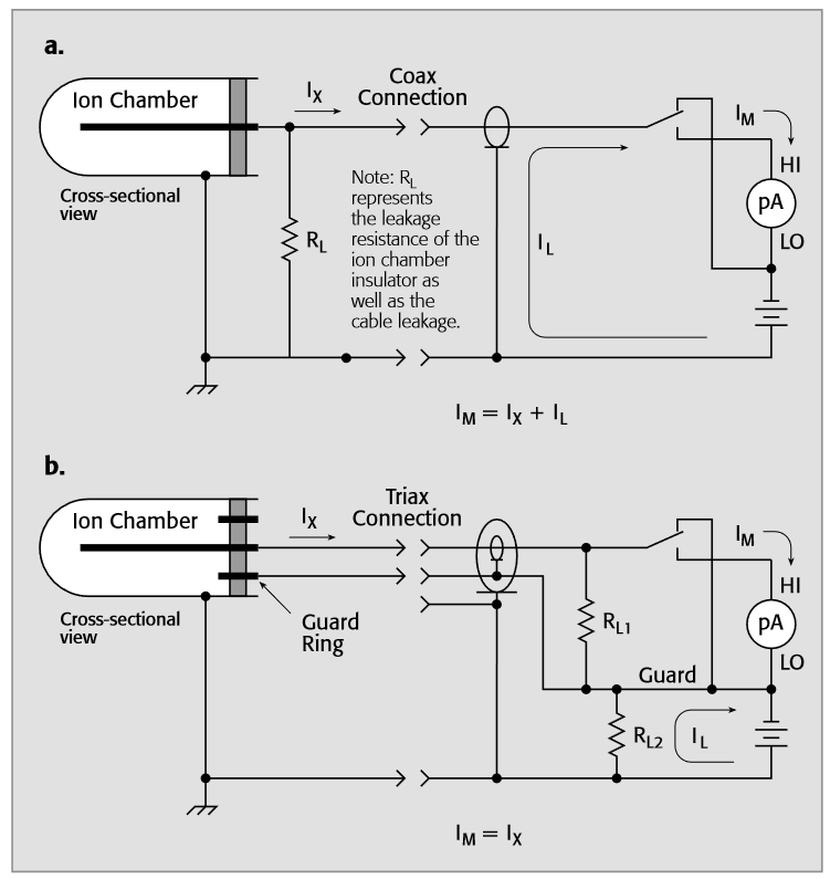
Another way to reduce leakage current due to cabling and test fixturing is to use guarding. By definition, a guard is a low impedance point in the circuit that is nearly at the same potential as the high impedance input terminal. Figure 14 shows an example of guarding as applied to switching an ion chamber to an ammeter (pA) to measure the ion chamber current (IX). An unguarded ion chamber is shown in Figure 14a. The circuit shows that the full bias voltage appears across the insulator leakage resistance (RL), so a leakage current (IL) will be added to the measured ion current (IM = IX + IL). The leakage resistance (RL) is due to the insulator of the ionization chamber and the coax cable insulation.
In Figure 14b, a guard ring is added to the ionization chamber. This guard circuit splits the leakage resistance into two parts. The coax connections of Figure 14a have been replaced with triax connections. The voltage across RL1 is the picoammeter voltage burden, normally less than 1mV, so the resulting leakage current will be quite small. The full bias voltage appears across RL2 (the leakage resistance between the inside and outer shields of a triax cable). However, the resulting leakage current does not flow through the meter, so it is not added to the measurement.
Guarding may also be necessary to prevent leakage current in low current test fixturing.
Electrostatic Interference
Shielding is required because high impedance circuitry is susceptible to pickup of spurious radiated noise. Relay contacts should be shielded from the coil to minimize induced noise from the relay power supply. The DUTs and interconnect cabling should also be shielded to prevent noise pickup. Any good conductor can be used as a shield. All shields should be connected to circuit LO.
Triboelectric Currents
Triboelectric currents are generated by charges created by friction between a conductor and an insulator, such as between the conductor and the insulation of a coax cable. This noise source can be reduced by using special low noise cable that has a conductive coating (such as graphite) and securing the interconnect cabling to minimize movement.
Electrochemical Currents
Electrochemical currents are generated by galvanic battery action caused by contamination and humidity. Thorough cleansing of joints and surfaces to remove electrolytic residue, including PC etchants, body salts, and processing chemicals, will minimize the effect of these parasitic batteries.
Settling Time
When a relay opens or closes, there is a charge transfer (on the order of picocoulombs), which causes a current pulse in the circuit. This charge transfer is due to the mechanical release or closure of the contacts, the contact-to-coil capacitance, and the stray capacitance between signal and relay drive lines. After a relay is closed, it’s important to allow sufficient settling time before taking a measurement. This time can be as long as several seconds. If a step voltage is applied to the circuit, a transient current is generated. This current will gradually decay to a steady value. The time needed to reach the steady value, or the settling time, can be used to determine the proper delay time for the measurement. See Keithley’s Low Level Measurements Handbook for more detailed discussions of generated currents and guarding.
Low Current Matrix Switching
Some low current applications require switching through a matrix. This is often the case when switching several Source-Measure Units (SMUs) to multipin devices or wafer level semiconductor measurements. All the special techniques used to minimize interferences for low current multiplexing also apply to low current matrix switching. However, offset current and leakage current are the types of interference most frequently encountered. In general, low current matrix switching can become complex and is best explained by illustration.
Figure 15 shows three SMUs from the Model 4200-SCS Semiconductor Characterization System connected through a two-pole matrix (Model 7174A Low Current Matrix Card) to a multipin device. Notice that the FORCE terminal of each SMU is connected to the HI terminal of the switch and the Guard of the SMU is connected to the Guard terminal of the switch. In this example, guarding becomes important to avoid leakage currents because the FORCE terminal of the SMU is at the test potential. With the guard terminal at the same potential, the leakage current through the switch is minimized. Guarding will also speed up the response time. The ground terminal (GNDU) of the Model 4200-SCS is connected to a single row of the matrix.
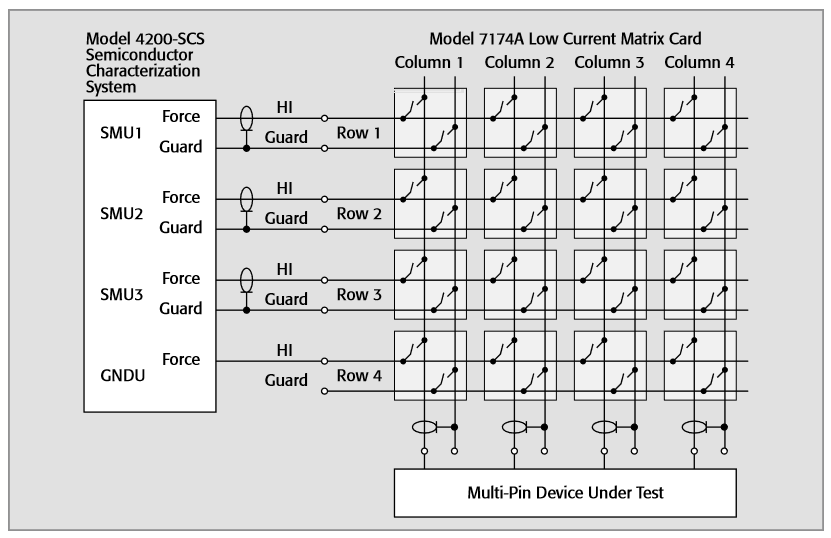
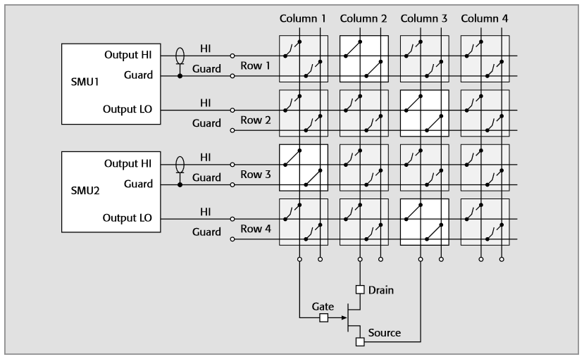
Figure 16 shows two independent SMUs with the Output LO terminals connected to separate rows. Note that each pin of the device under test, the FET, is connected to a single column. The guard terminals of the matrix card are not connected to the device. To connect the SMUs to the transistor, close crosspoint Row 1/Column 2 to connect SMU1 to the drain, Row 3/Column 1 to connect SMU2 to the gate, and Row 2/Column 3 and Row 4/Column 3 to connect both SMU Output LO terminals to the source terminal of the FET.
Remote sensing may be necessary if the current through a given path is high enough to cause a significant voltage drop. Remote sensing compensates for test lead and switch voltage drops and ensures that the programmed output voltage of the SMU is delivered to the load. Remote sensing allows making accurate load voltage measurements. Figure 17 shows SMU1 connected to four rows to enable remote sensing, thereby allowing accurate measurement of the collector-emitter voltage of the BJT. SMU2 is used to supply the relatively small base current and requires only two rows. To connect SMU1 between the emitter and the collector, close crosspoints Row 1/Column 4, Row 2/Column 5, Row 3/Column 2, and Row 4/Column 1. Note that remote sensing requires the use of four rows and four columns. To connect SMU2 between the base and the emitter, close crosspoints Row 5/Column 3 and Row 6/Column 1. Remote sense is not needed to source the base current because the lead resistance does not affect the current.
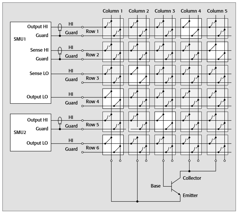
When connecting two SMUs in a matrix, the Output LO terminals of both SMUs can be tied together and connected to the device using one row.However, the SMU in remote sense may be outputting high current (>1mA) and the resulting voltage drop may interfere with the second SMU if it is used to measure small voltages (<1mV).
Once a given combination of matrix cards, sourcing, and measuring devices is put together, it may be desirable to measure the offset current for various pathways to characterize the system. To measure the offset current, close a specific crosspoint and use an electrometer or SMU to measure the current with everything in place except the device under test.Periodically perform this system check on only the crosspoints for low current switching. If the offset current is relatively constant, this value can then be subtracted from subsequent measurements. Leakage current is another source of measurement interference that must be characterized.It is dependent on the applied voltage, contamination, and humidity.
Leakage current can be determined from path to ground or from path to path. The leakage current can be determined by applying a known voltage and measuring the current between either path to ground or path to path. Once the leakage current in a given pathway is known and remains consistent, it can be subtracted from subsequent measurements.However, humidity and contamination may change the leakage current value over time, so it must be characterized periodically.
Matrix cards suitable for these applications include Models 7152, 7072, and 7174A. All connections should be made with triax cables. Low current matrix cards usually use triax connections to eliminate a possible shock hazard from the guard voltage. Note the outer shield is always at earth ground potential and has been omitted from these figures for clarity.
Resistance Switching
Switching an ohmmeter to a device under test is common to a variety of applications, including measuring the insulation resistance of materials, continuity testing of cables and connectors, contact resistance measurements, and measuring the resistance of components such as resistors, thermistors, and potentiometers.
Resistance measurements may range from less than 1Ω to greater than 1012Ω, so the switching techniques required may vary significantly based on the magnitude of the resistance. Low resistance measurements are generally those less than 100Ω, mid-range are those from 100Ω to 107Ω, and high resistance measurements are those greater than 107Ω. As with any measurement, the exact point at which low resistance techniques should be used depends upon the desired measurement accuracy. For example, a 1ppm measurement of a 1kΩ resistor implies an uncertainty of less than 1mΩ, which can only be achieved by using a four-wire technique.
For scanning resistances in the mid-range (100Ω to 10MΩ), either singleended (one-pole) or differential (two-pole) methods can be used. The single-ended method is shown in Figure 18a. Note that all the resistors under test have a common terminal that is connected to meter low.
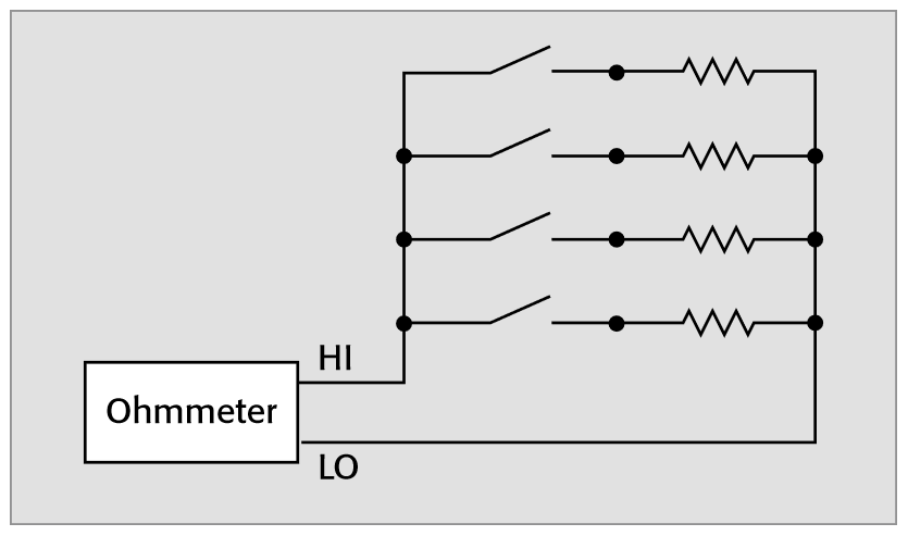
Figure 18b illustrates the differential method. A two-pole relay is used to connect both terminals of the unknown resistor to the meter.
The application usually dictates whether the single-ended or differential method should be used for switching. The advantage of the single-ended method is that it requires only half as many switches as the differential method. The only advantage of the differential method is that the offset voltages of the two switches tend to cancel each other. However, given that these are microvolt-level voltages, the differential method is not usually an issue for mid-range resistance switching.
Low Resistance Switching
Applications such as contact resistance measurements and cable continuity testing typically involve switching low resistances. Low resistance (<100Ω) switching requires using techniques that are normally unnecessary for mid-range or high resistances. Offset compensation and remote sensing are techniques often used to eliminate errors due to the switch contact resistance.
Offset Compensation
Spurious microvolt level signals are often present in low resistance circuits, most often as a result of thermoelectric effects. If dissimilar metals are present, a temperature differential across the circuit can easily add several microvolts to the measurement circuit. Switches in the circuit may also add up to several microvolts of error voltage to the measurement. This error voltage is known as contact potential or offset voltage.Offset compensation will eliminate the switch contact potential, as well as any thermoelectric voltage offsets in the entire measurement circuit.
Offset compensation requires making two voltage measurements with two different but known currents. Most often, the second current is of the same magnitude but opposite polarity as the first. The resistance is calculated by dividing the difference between these two voltage measurements by the difference between the two source currents. This procedure will cancel the offsets. In applications where timing is critical, offset compensation may not be practical, because it takes twice as long to make a measurement.
Some DMMs provide a built-in offset compensation capability. Two measurements are made, one at a positive current and another at nearly zero current. The DMM then calculates the resistance automatically.
Four-Wire Switching
Accurate measurements of low resistance in a system require a four-wire connection to eliminate both lead wire and switch contact resistance.Figure 19 is an example of four-wire switching. In this diagram, two of the leads (HI and LO Source) supply current to the resistors, while the other two leads (HI and LO Sense) measure the voltage developed across the resistors. The source leads are connected to one bank of switches and the sense leads are connected to the other bank of switches.
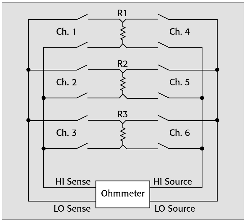
To measure the resistance of the first resistor (R1), channels 1 (Ch. 1) and 4 (Ch. 4) are both closed. The actual resistance measurement is made with either a DMM or a micro-ohmmeter with four-wire ohms capability, with a separate current source and voltmeter, or with a single sourcemeasure instrument.
As shown in Figure 19, two sets of two-pole relays are used for low resistance switching. The poles in an individual relay will have similar offset voltages. By using these two poles to connect the low voltage signal to the sense terminals of the meter, the offset voltages or the contact potential (as it is specified), will tend to cancel each other. When the sense leads are connected through two different relays to the unknown resistor (R), as shown in Figure 20a, the offsets are not likely to cancel and may actually combine to cause an even greater error. Even a properly connected two-pole switch, like that shown in Figure 20b, will have some differential offset voltage that will not cancel out. The error caused by such offset voltage can be virtually eliminated by using offset compensation.
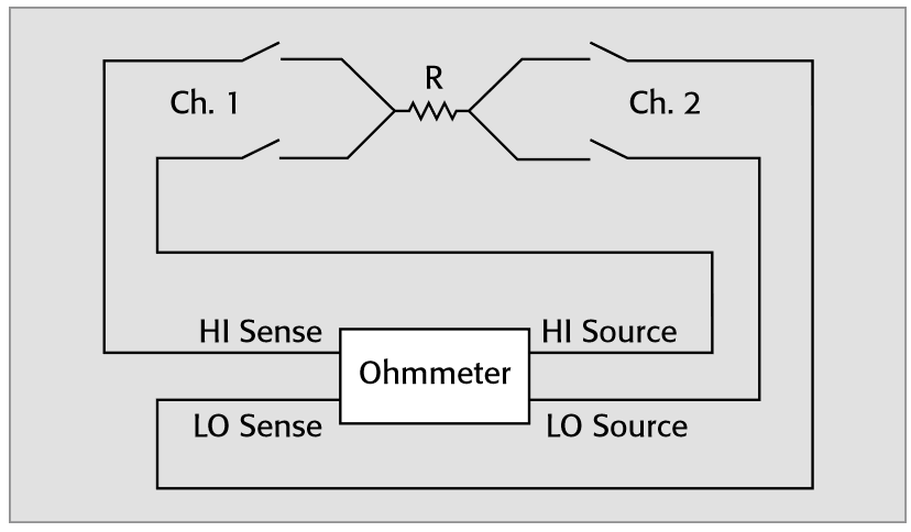
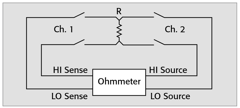
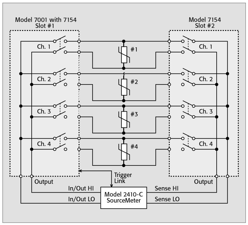
Figure 21 shows an example of the preferred connection scheme when testing metal-oxide varistors. The Model 2410-C SourceMeter® instrument is ideal for testing MOVs because of its ability to source up to 1100V at 21mA. One Model 7154 High Voltage Card connects the source lines to the devices and another Model 7154 connects the sense lines. The twopole relays minimize lead resistance and voltage drop in the switch. This is particularly important when measuring relatively small voltages (millivolts).
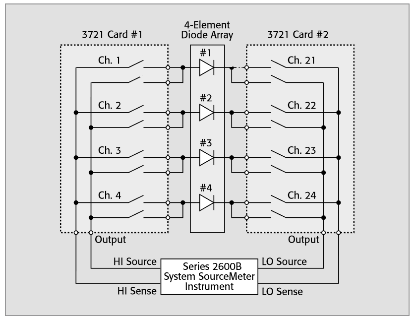
On the other hand, the example of Figure 22 minimizes lead resistance only. With the HI leads and LO leads on the same two-pole relays, offset voltages in the Model 3721 multiplexer switches will not cancel each other because very little current flows in the high impedance sense leads.Depending on the needs of the application, the offset voltages can be addressed with the offset-compensated ohms feature of the Series 2600B System SourceMeter instrument.
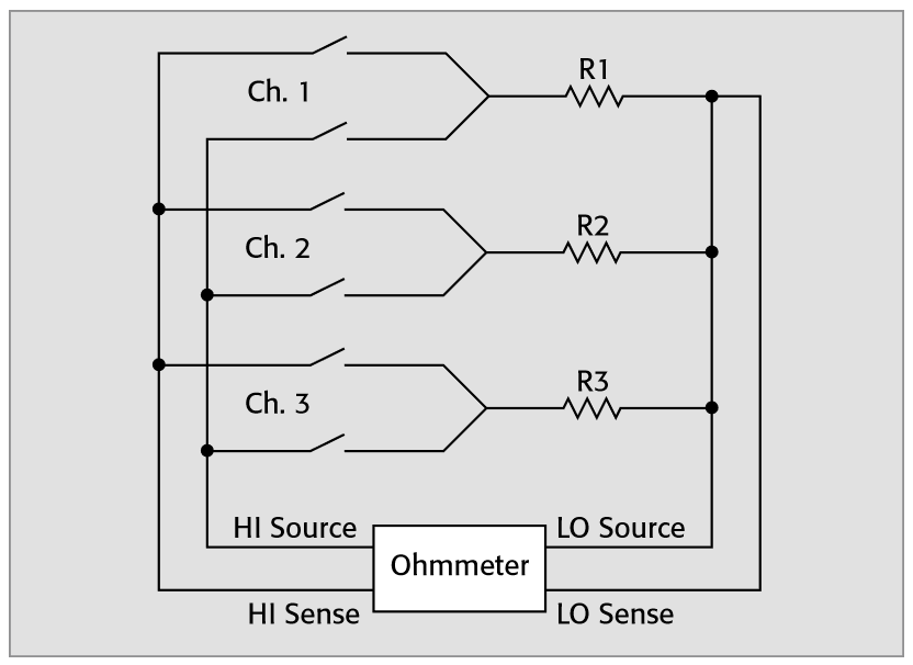
In some applications, the resistances to be tested may have a common terminal. In this case, only one two-pole switch per resistor is necessary, as shown in Figure 23. This approach has the advantage that only half as many switches are required, so it is more economical. The disadvantage is that the offset voltage of the single pole in the sense circuit is added to the measurement. Switching only a single sense lead will not cancel the offset voltage as happens when both sense leads are switched through the same two-pole relay. However, offset compensation will generally correct for this error source at the cost of increased measurement time. Some ohmmeters provide this feature, including two Keithley product configurations, the Model 2700 DMM/Switch Mainframe with the Model 7701 32-Channel Differential Multiplexer Card and the Model 3706A System Switch/ DMM with the Model 3721 Dual 1×20 Multiplexer Card. This feature is known as "common side ohms." When operating in common side ohms mode, each instrument has the ability to recognize the appropriate card and convert the two-wire connection into a four-wire measurement.
Other Issues
Some low resistance applications may require sourcing a relatively high test current and measuring very low voltages. This may require using a high current switch card for sourcing and a low voltage switch card for measuring.
When switching low impedances, shielding needs are minimal. Shielding is generally needed only in electrically noisy environments.
High Resistance Switching
Applications such as measuring capacitor leakage, multi-conductor cable insulation resistance, and pin-to-pin leakage of connectors require measuring high resistances through switches. Special techniques are required for switching resistances greater than 10MΩ. Different high resistance switching techniques will be needed, depending on whether the source voltage/measure current or the source current/measure voltage method of determining resistance is used. However, techniques such as shielding and guarding apply to both methods.
Source Voltage/Measure Current Method
This technique for measuring high resistance involves sourcing a known voltage, measuring the resulting current, and calculating the resistance.As shown in the schematic in Figure 24, one side of each resistor is connected through a set of switches to the picoammeter (pA), while the other end is connected through a second set of switches to a DC voltage source. To measure the resistance of R1, close switches Ch. 1 and Ch. 4.
If the measured current is less than 100nA, the switches used to connect the resistors to the picoammeter must have low offset current and high isolation resistance. In many cases, a Form C switch is preferred. The Form C switch keeps one end of the device under test at guard potential (approximately 0V) when the switch is de-energized. This prevents leakage current across the relay that would degrade the measurements. The Form C switch also allows the device under test to be charged for a controlled time interval before measuring.
General-purpose switches are usually sufficient for switching the voltage source unless high voltages (>100V) are involved, in which case, high voltage switch cards are necessary. If high voltage is used, current limiting resistors are needed to avoid damage to the current switches in case the device under test breaks down. The current limiting resistor (R) is placed in series with the device under test. The value of this resistor is chosen such that, in the event of device failure, the short circuit current will not exceed the maximum current specification of the relays on either set of switch cards. The voltage rating of these resistors must be at least equal to the test voltage.
In some cases, the device under test may have a common terminal, as shown in Figure 25. In this case, the voltage source will be applied to all the devices simultaneously. As a result, the excitation voltage time is different for each resistance to be measured. This will cause errors for some time-dependent applications, such as measuring insulation resistance or capacitor leakage. In these cases, the measured resistance is a function of the excitation time.
When the measured current is large compared to the relay current offset specification, then Form A switches can provide a more economical solution, as shown in Figure 26. In this example, the leakage current of all open relays will contribute to the measured current. Unfortunately, this leakage current cannot be guarded. Also, if there is a leakage path between devices (as when measuring the insulation resistance between traces on a circuit board or multi-conductor cable), this will also degrade measurement accuracy. In this diagram, each of the resistors has one end connected together to the voltage source. In this case, voltage source switching is unnecessary, because the device under test cannot be pre-charged.
Special techniques must be used to minimize interferences such as offset currents, leakage currents, electrostatic interference, triboelectric currents, and electrochemical currents. These sources of errors may be due to the switch card or the connecting test fixturing.
Source Current/Measure Voltage Method
In some cases, high resistance is measured by sourcing a current and measuring the resulting voltage. Although this is not the preferred method for measuring high resistance, it is necessary for some applications, such as van der Pauw resistivity measurements of semiconductors.High impedances are being switched, so some of the same switching techniques used when switching low current and high impedance voltages are equally applicable here. To avoid errors, choose a card with low offset current and high isolation resistance. Shielding is necessary to prevent noise due to electrostatic interference.
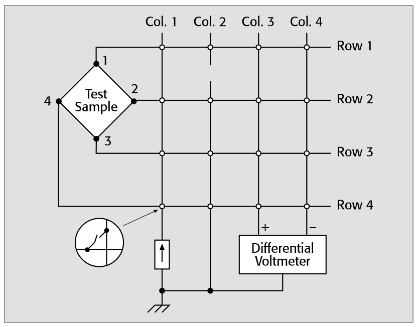
Figure 27 shows a simplified van der Pauw resistivity measurement with a current source and a differential voltmeter. By closing crosspoints Row 1/Column 1 and Row 2/Column 2, the current source is connected to sample terminals 1 and 2. Closing crosspoints Row 3/Column 3 and Row 4/Column 4 will connect the voltmeter between terminals 3 and 4. For more detailed information on van der Pauw resistivity measurements, consult Keithley's Low Level Measurements Handbook.
Signals Involving Reactive Loads
Switching circuits that include reactive elements need special care to avoid problems due to transient effects. The methods used to limit transient effects depend on whether the load is capacitive or inductive. When a capacitive load is connected through a switch to a voltage source, the in-rush current may exceed the current rating of the switch and weld the contacts shut. As Figure 28a indicates, when the switch (S) is closed, the peak current (i) is limited mainly by the sum of the wiring resistance and the relay contact resistance. The peak current may exceed the current rating of the relay and cause welding of the contacts. Cold switching is the most effective way to prevent this current surge. If cold switching is impractical, it may be possible to add series resistors to limit the current to a safe value, as shown in Figure 28b. The value of the series resistor (R) should be greater than the ratio of the applied voltage to the maximum current rating of the switch card. However, if the resistor is too large, it may affect measurement accuracy. The current surges of these two circuits are illustrated in Figure 28c.

Capacitor leakage measurements and insulation resistance measurements of multi-conductor cables are two applications where switching capacitive loads may be a particular problem. Even with resistive loads, the capacitance of a shielded connecting cable may cause relay welding. In this case, the series resistor should be placed as close to the relay as possible to limit the current when charging the cable capacitance.
When an inductive load is connected to a voltage source, the current will increase relatively slowly. However, when the switch is opened, a large inductive reaction voltage will appear across the switch contacts and may damage the contacts. The contact bounce that occurs on closure can also produce an inductive reaction voltage, because the current is nterrupted repeatedly. A voltage-clamping device across the inductive load is usually required. Figure 29 illustrates four possible circuits for voltage clamping. For best results, the voltage-clamping device should be located near the load.

RF and Microwave Switching
Given the explosive growth of the communications industry, a tremendous amount of testing is being performed on the various components that make up different communications systems. These components range from active components such as Radio Frequency Integrated Circuits (RFICs) and Microwave Monolithic Integrated Circuits (MMICs) to complete communication systems. While the testing requirements and procedures for these components differ widely, all are tested at very high frequencies, typically in the gigahertz range. The main components in a test system may include DC bias, DC measurement, RF power meter, network analyzer, RF sources, and other instruments. Automating the test process and improving test efficiency demands integrating RF/microwave and low frequency switching systems into the test system.
Microwave Switch Types
Available microwave switch configurations include a simple single-pole double throw (SPDT) switch, multi-position switch, matrix, and cascade.
An SPDT switch has one input port, which can be connected to one of two output ports. A multi-position switch connects one input port to one of several output ports. Keithley’s System 46 can accommodate eight SPDT coaxial microwave relays and four multi-pole coaxial microwave relays.
A matrix switch can connect any input to any output. Two types of matrices are used in microwave switching: blocking and non-blocking. A blocking matrix connects any one input to any one output. Other inputs and outputs cannot be connected at the same time. A non-blocking matrix allows multiple paths to be connected simultaneously through the matrix.
The cascade switch configuration is an alternate form of multi-position switch. The cascade switch connects one input to one of many outputs using multiple relays. The path length (and therefore, the phase delay) varies, depending on the number of relays that the signal must go through.
RF Switch Card Specifications
The use of a switch will inevitably degrade the performance of the measurement system, so it is important to consider several critical parameters that may affect system performance significantly. During the design phase, the costs and benefits are often weighed against each other to achieve an optimal solution. When choosing an RF switch system, some of the critical electrical specifications to review include crosstalk (path isolation), insertion loss, voltage standing wave ratio (VSWR), and bandwidth.
RF Switch Design Considerations
When designing an RF switch system, additional factors that may affect switch system performance include impedance matching, termination, power transmission, signal filters, phase distortion, and cabling.
Impedance Matching: Given that the switch is positioned between the measurement instruments and the DUT, matching the impedance levels of all elements in the system is critical. For optimal signal transfer, the output impedance of the source should be equal to the characteristic impedance of the switch, the cables, and the DUT. In RF testing, the most commonly used impedance levels are 50Ω and 75Ω. Whichever impedance level is required, proper matching will ensure the overall system integrity.
The input VSWR and signal path VSWR determine the limitation on the accuracy of the measurement:
Mismatch Uncertainty (dB) = 20 × log (1 ± Гsig pathГinstr)
| Г = | VSWR - 1 |
| VSWR + 1 |
If both the signal path output and the instrument input have good VSWRs of 1.3:1 at a frequency, then the uncertainty due to mismatch alone is ±0.15dB.
Termination: At high frequencies, all signals must be properly terminated or the electromagnetic wave will be reflected from the terminating point.This, in turn, will cause an increase in VSWR. An unterminated switch increases VSWR in its off condition, while a terminated switch will try to provide a 50Ω match on or off. The VSWR increase may even damage the source if the reflected power is large enough. All paths through a system must be terminated with their characteristic impedance.
Power Transmission: Another important consideration is the system's ability to transfer the RF power from instrument to DUT. Due to insertion loss, the signal may require amplification. In other applications, it may be necessary to reduce the signal power to the DUT. An amplifier or attenuator may be needed to ensure that the required level of power is transmitted through the switch.
Signal Filter: Signal filters can be useful in a number of circumstances, such as when spurious noise is inadvertently added to the signal as it travels through the switch. They can also be helpful if the original signal frequency does not fit in the DUT testing frequency. In these cases, filters can be added to the switch to modify the signal frequency bandwidth, or spurious signals at unwanted frequencies can be eliminated from the signal to the DUT.
Phase Distortion: As the size of a test system expands, signals from the same source may travel to the DUT via paths of different lengths, resulting in phase distortion. This specification is often referred to as propagation delay. For a given conducting medium, the delay is proportional to the length of the signal path. Different signal path lengths will cause the signal phase to shift. This phase shift may cause erroneous measurement results. To minimize phase distortion, keep the path lengths the same.Taking all of these design considerations into account when configuring an RF/microwave switch system can be simplified by ordering a package solution, such as the System 46 RF/Microwave Switch System.It can be configured with up to 32 channels for controlling microwave switches. It also tracks contact closures for proactive maintenance of relays, and performance parameters, such as VSWR or insertion loss, for trend analysis.
Digital Switching
High speed digital signals exhibit RF behavior in real-world devices, which creates a need for RF or microwave components when routing these signals in test systems. Digital (and optical) engineers must be aware of RF parameters in product development and production testing
Digital Design Considerations
The first consideration when switching digital signals is providing adequate bandwidth to preserve the frequency harmonics of the digital pulse and their power spectral distribution. The switching solution should have as a minimum the bandwidth of the DUT, and preferably equal to the bandwidth of any higher frequency source and measurement equipment.
Because the -3dB specifications of switch cards are based on sinewave signals, an approximation is needed for square waves.If the frequency of the square wave is known, the required bandwidth is determined by the highest harmonic that needs to pass without distortion, whether that is the third, fifth, seventh, or higher harmonic.
If the frequency of the square wave is unknown, the following equation approximates the minimum bandwidth for digital signals:
| Bandwidth (Hz) = | 0.35 |
| risetime (s) |
Digital switching has some other considerations in addition to those listed in the section for "RF Switch Design Considerations":
Arcing: The RF I (radio frequency interference) generated by high voltage switching may disrupt high-speed logic circuits.
Hot switching: When digital signals are being switched, they may change state with any length of power interruption. Using hot switching prevents digital state changes.
Make-before-break: Use Form A isolated switches instead of Form C relays to allow for make-before-break operation.
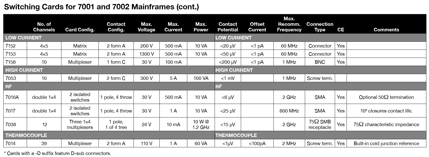
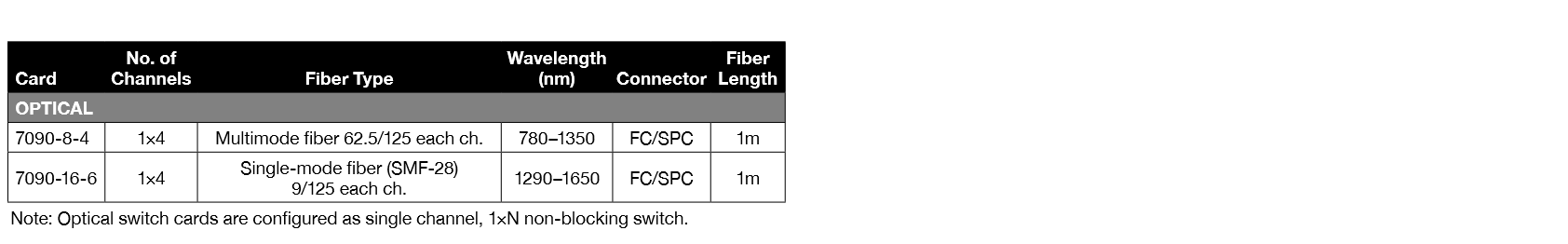
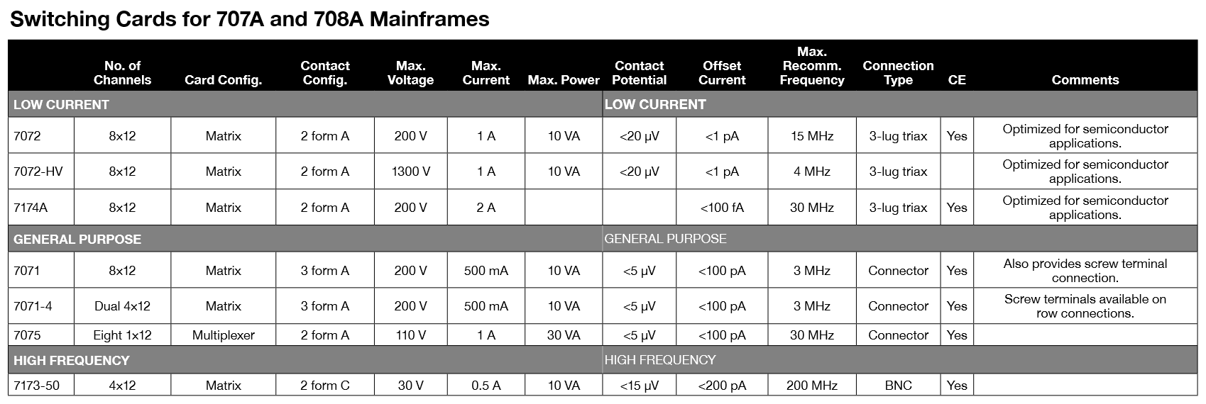
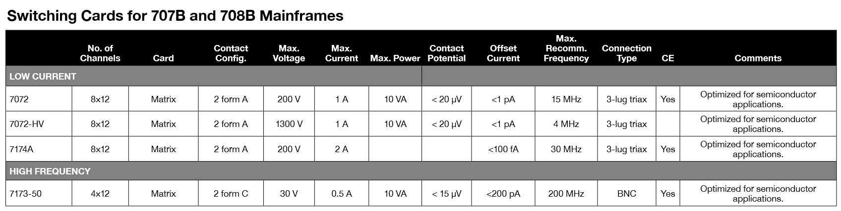
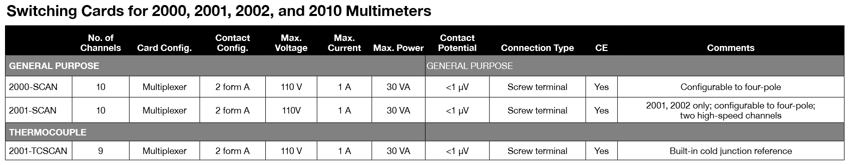
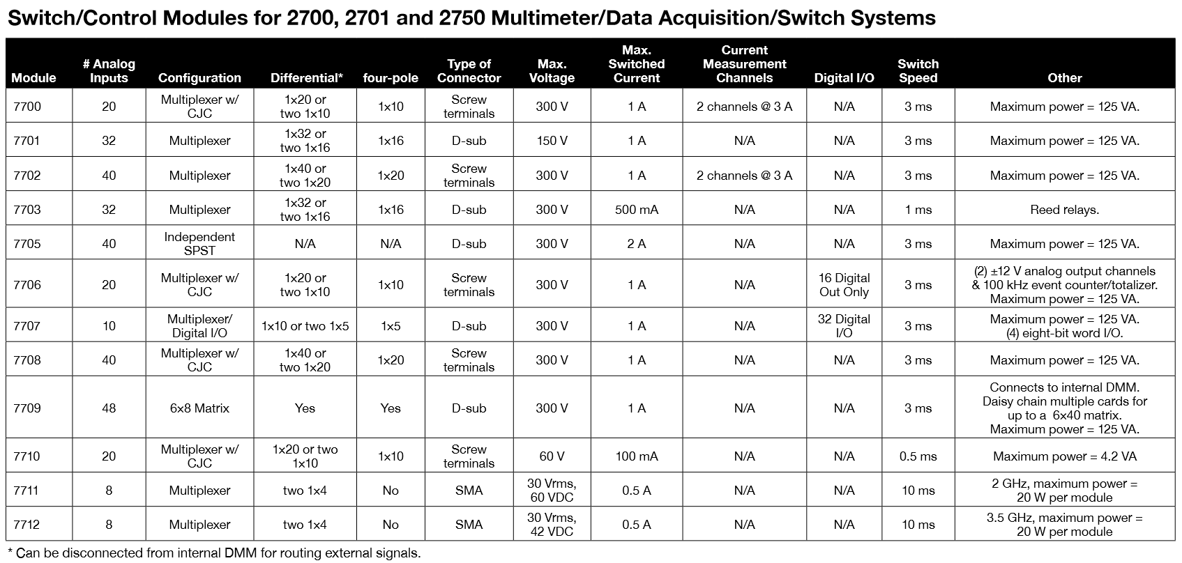
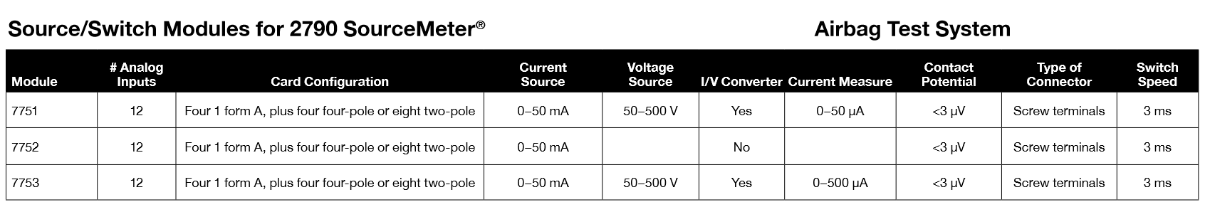
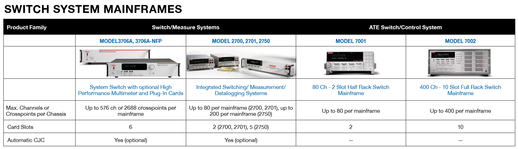
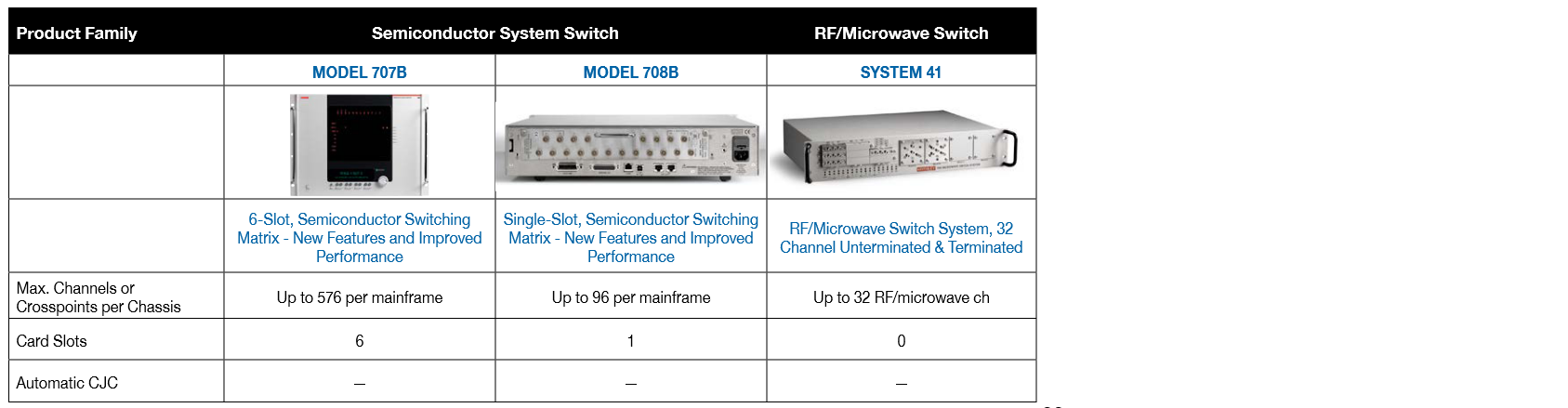
Switch Card and Switch Module Selector Guides

Find more valuable resources at TEK.COM
Copyright © Tektronix. All rights reserved. Tektronix products are covered by U.S. and foreign patents, issued and pending. Information in this publication supersedes that in all previously published material. Specification and price change privileges reserved. TEKTRONIX and TEK are registered trademarks of Tektronix, Inc. All other trade names referenced are the service marks, trademarks or registered trademarks of their respective companies.
No.3146 10.13