Current Language
×
Japanese (Japan)

言語の選択:

トグル・メニュー
Current Language
×
Japanese (Japan)

言語の選択:

ダウンロード

マニュアル、データシート、ソフトウェアなどのダウンロード:

ダウンロード・タイプ
型名またはキーワード

フィードバック

オシロスコープを使用した電源スイッチング損失の測定

Measuring Switching Loss with an Oscilloscope

はじめに

バッテリー駆動デバイスの使用時間を延ばし、電力効率を向上させる需要が高まる中、電力損失を分析し、電源効率を最適化する能力が以前にも増して重要になっています。効率における鍵となる要素の一つは、スイッチングデバイスでの損失です。通称「スイッチング損失」です。

このアプリケーションノートは、スイッチング損失の測定と、オシロスコーププローブを使用してより良く、より再現性のある測定を行うためのいくつかのヒントを簡単に概説します。

典型的なスイッチングモード電源の効率は約87%であり、入力電力の13%が電源内で散逸しており、そのほとんどは廃熱としてです。この損失のうち、かなりの部分が通常MOSFETsやIGBTsなどのスイッチングデバイスで散逸しています。

理想的には、スイッチングデバイスは「オン」または「オフ」の状態であり、電灯のスイッチのようにこれらの状態間を瞬時に切り替えます。「オン」状態では、スイッチのインピーダンスはゼロであり、どれだけの電流が流れていてもスイッチで電力は散逸しません。「オフ」状態では、スイッチのインピーダンスは無限大であり、電流は流れていないため、電力は散逸しません。

LIV curves
図1. 簡略化されたスイッチングモード電源のスイッチング回路

実際には、「オン」(導通)状態でもいくらかの電力が消費され、しばしば、「オン」と「オフ」(遮断)の間、および「オフ」と「オン」(通電)の間の遷移時に、さらに多くの電力が消費されます。

LIV curves
図2. スイッチングデバイスにかかる瞬時電圧とそのデバイスを流れる瞬時電流を乗算することで、スイッチングサイクル全体を通じた瞬時電力が得られます。

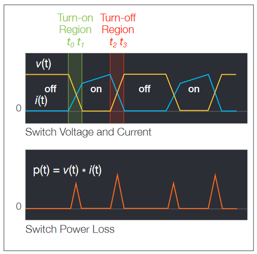
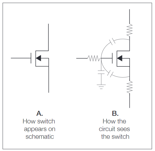
これらの非理想的な振る舞いは、回路内の寄生要素によって発生します。図3のBに示されているように、ゲートに存在する寄生容量はデバイスのスイッチング速度を遅らせ、オンとオフの時間を長くします。MOSFETのドレインとソースの間の寄生抵抗は、ドレイン電流が流れているときに常に電力を消費します。

LIV curves
図3. A:スイッチが回路上でどのように表されるかを示した図  B:回路がスイッチをどのように認識するかを示した図

導通損失

導通状態では、スイッチには小さな抵抗とそれを通過する電圧降下があり、流れる電流の関数としてスイッチは電力を消散します。

MOSFETの場合、この電力は通常以下のようにモデル化されます:

P = ID2 * RDSon = ID * VDS

- IDはドレイン電流を表しています

- RDSonはドレインとソース間の動的オン抵抗で、しばしば1W未満です

- VDSはドレインとソース間の飽和電圧で、しばしば1V未満です

IGBTやBJTの場合、この電力は通常以下のようにモデル化されます:

P = IC * VCEsat

- IC はコレクタ電流を表しています

- VCEsat はコレクタとエミッタ間の飽和電圧を表し、しばしば1V未満です

ターンオン損失

通電時には、スイッチを通る電流が急速に増加し、デバイスを通る電圧降下がすばやく減少します。しかし、MOSFET内のゲートからドレインへの寄生容量などの寄生要素が、スイッチが即座にオンになるのを防ぎます。デバイスが通電している間、デバイスを流れる電流とデバイスにかかる電圧が大きく、大きな電力損失が発生します。

MOSFETの場合、通電時のこの電力は通常以下のようにモデル化されます:

P = ID * VDS

- ここで IDはドレイン電流を表しています

- VDSはドレインとソース間の電圧を表します

IGBTやBJTの場合、通電時にこの電力は通常以下のようにモデル化されます:

P = IC * VCE

- IC はコレクタ電流を表しています

- VCE はコレクタからエミッタへの電圧を表します

ターンオフ損失

通電時と似た方法で、遮断時にはスイッチを流れる電流が急速に減少し、デバイスを通る電圧降下が急速に増加しますが、回路の寄生要素がスイッチの瞬時の遮断を防ぎます。デバイスが遮断されている間、デバイスを流れる電流とデバイスにかかる電圧は大きく、大きな電力損失が発生します。上記の方程式も適用されます。

スイッチング損失の測定方法

スイッチング損失を測定する方法には2つのアプローチがあります。一つはマニュアルセットアップとオシロスコープの組み込み測定を使用する方法、もう一つはいくつかのオシロスコープで利用可能な自動測定システムを使用する方法です。自動測定には設定が簡単で、繰り返し結果を容易に得られるという利点があります。いずれの技術を使用する場合も、慎重なプロービングと最適化が良い結果を得るのに役立ちます。

プロービングと測定セットアップ

特定の電力測定について議論する前に、正確で再現性のある測定を行うための六つの重要なステップがあります。

1. 電圧オフセット誤差を取り除く:差動プローブ内のアンプにはわずかなDC電圧オフセットが存在する可能性があり、これが測定精度に影響を与えます。入力を短絡し、シグナルを適用せずに、プローブ内のDCオフセットを自動的または手動でゼロに調整します。

2. 電流オフセット誤差を取り除く:電流プローブには、プローブ内の残留磁気やアンプのオフセットによるDCオフセット誤差が生じることがあります。クランプを閉じてシグナルを適用せずに、プローブ内のDCオフセットを自動的または手動でゼロにします。

3. タイミング誤差を取り除く:瞬時電力測定は複数のシグナルに基づいて計算されるため、これらのシグナルが適切に時間同期されていることが重要です。電圧と電流を測定するために異なる技術が使用され、これらのデバイスを通る伝播遅延が大きく異なる可能性があり、これが測定誤差を引き起こすことがあります。良好な結果は、一般にデスキューメニューで名目上の伝播遅延の差を考慮してインターチャネルタイミングを調整することによって得られます。最も正確な結果を得るためには、すべての入力に高スルーレートのシグナルを適用し、すべてのチャネル間の相対的なタイミングオフセット(スキュー)を慎重に取り除きます。

4. 信号対雑音比の最適化:すべての測定システム、特に現代のオシロスコープのようなデジタルデバイスでは、ノイズの影響を最小限に抑え、垂直分解能を最大化するために、信号を可能な限り大きく(クリッピングしない範囲で)保つことが良好な測定技術として要求されます。これには、信号をプロービングする際に必要最低限の減衰を使用することや、オシロスコープの全ダイナミックレンジを使用することが含まれます。

5. シグナルコンディショニング:入力シグナルのコンディショニングによっても、測定品質を向上させられます。帯域幅制限を使用して、関心のある周波数より上のノイズを選択的に減少させられますし、平均化を使用して、シグナル上の相関がない、またはランダムなノイズを減少させることができます。ハイレゾリューション取得モードは帯域幅制限とノイズ削減を提供し、垂直分解能を向上させるとともに、シングルショットモードで取得したシグナルに対しても機能します。

6. 精度と安全性:最高の精度を確保するためには、機器を通常の運用範囲内で使用し、ピークレーティング以下で使用することが重要です。また、安全のためには、常に機器の絶対最大仕様内で操作を行い、使用に関するメーカーの指示に従ってください。

スイッチング損失の測定 - マニュアルセットアップと組み込み測定

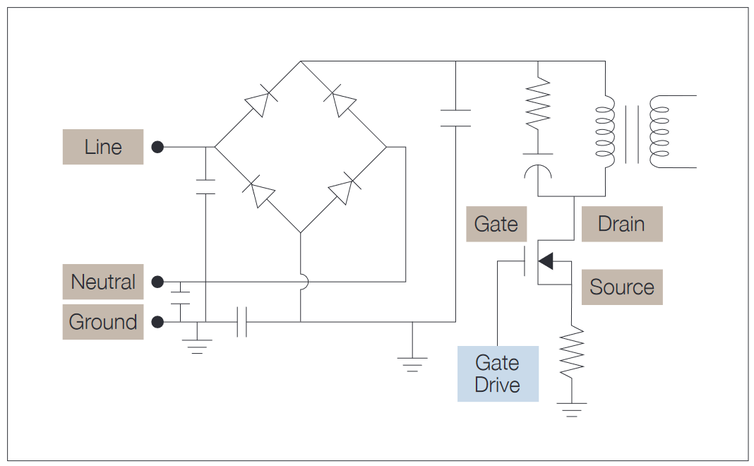
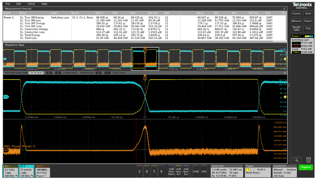
遮断損失を測定する一つの方法は、ゲート付き測定を使用します。目的は遮断フェーズ中に散逸する平均電力を測定することです。例えば図4では、MOSFETのVDSを差動電圧プローブで取得し、黄色で示されています。ドレイン電流はAC/DC電流プローブで取得され、シアン色(明るい青色)で表示されます。各チャネルの垂直感度とオフセットは調整され、信号が垂直範囲の半分以上を占めるようになっていますが、目盛の上端と下端を超えないようにしています。

LIV curves
図4. ウェーブフォームの乗算と、取得全体にわたる電力データの平均測定を使用したスイッチング電力損失測定。この技術は、オシロスコープの標準機能を使用したマニュアルセットアップに依存しています。

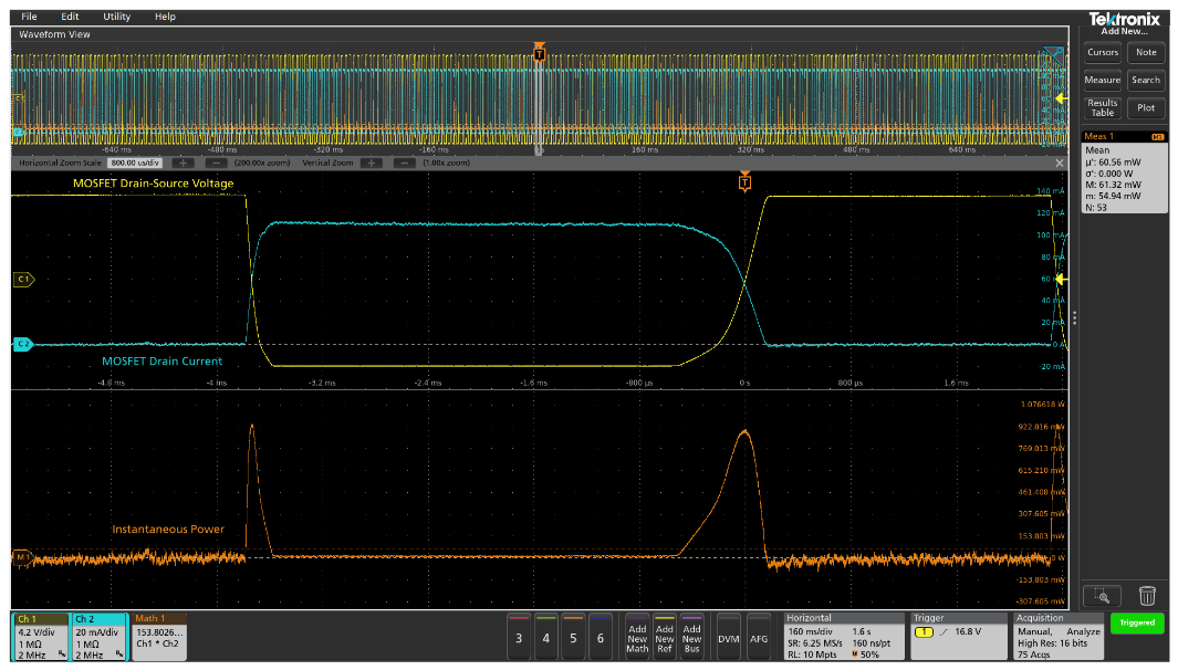
視覚分析において安定した表示が重要であるため、オシロスコープのエッジトリガーは電圧波形の50%点に設定されます。次に、信号のエッジの適切なタイミング分解能を確保するためにサンプルレートが設定されます。この場合、6.25 GS/sのサンプルレートを設定することで、スイッチング波形の各エッジに多くのサンプルポイントが得られます。最後に、ハイレゾリューション取得モードを有効にして、垂直分解能を16ビットに増加させます。

その後、波形数学を使用して電流と電圧を乗算し、オレンジ色の瞬時電力波形を作成します。自動測定を使用して、電力波形の代表値または平均値を測定します。

この例では、エンジニアは手動でオシロスコープを調整して、スイッチング損失測定の品質を最適化しました。後日、同じエンジニアまたは別のエンジニアが測定を少し異なる方法でセットアップする可能性は高く、その結果、測定結果が異なる可能性があります。そこで、電力分析ソフトウェアを通じて測定を自動化することで、多くの変動要因を排除できます。

スイッチング損失の測定 - 電力分析ソフトウェアを使用した自動測定

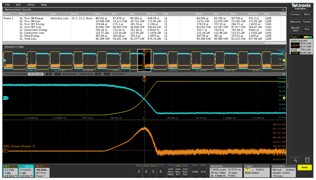
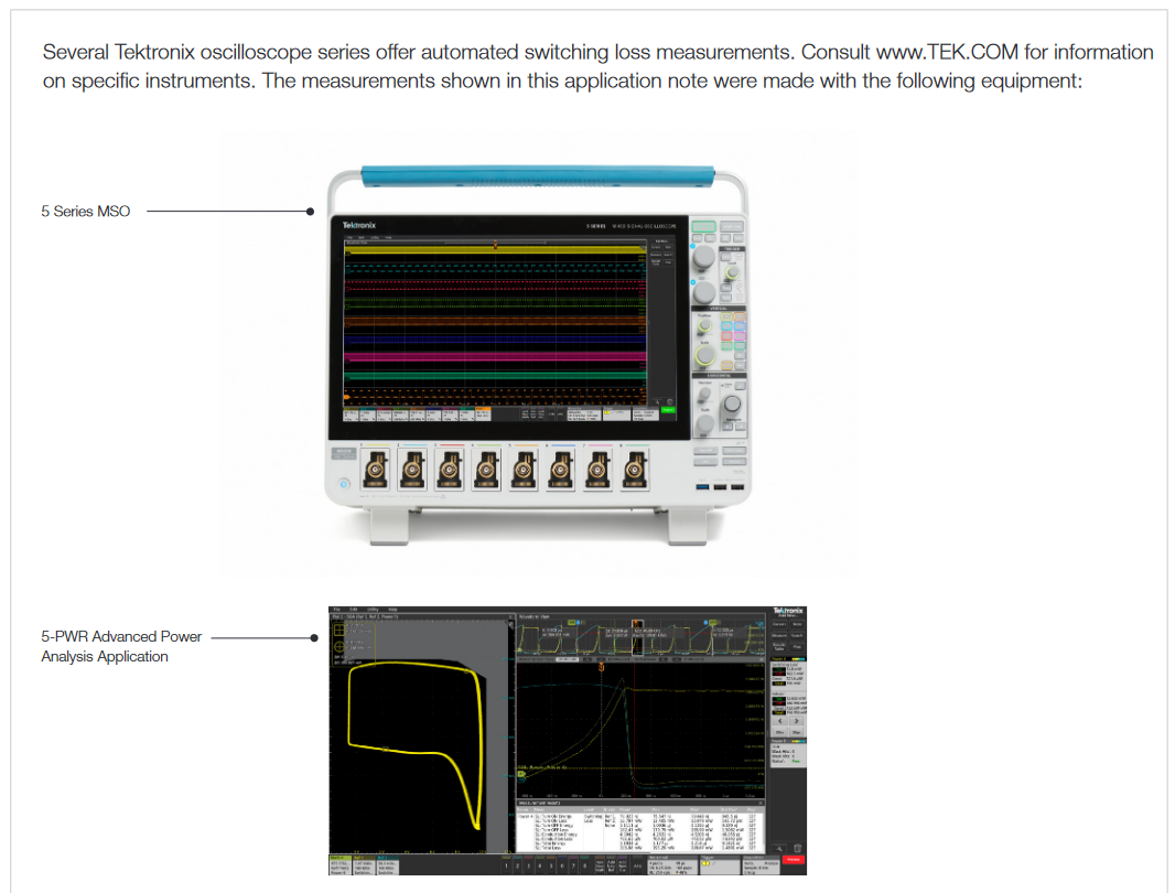
セットアップを一貫して最適化し、測定の再現性を向上させるために、電力測定アプリケーションが役立ちます。この場合、PWR Advanced Power Analysisアプリケーションはスイッチング損失測定のためのカスタムオートセットを提供し、ボタン一つでスイッチング損失の電力およびエネルギー測定の完全な一連の作業を実行します。

スルーレートとスイッチング損失

瞬時電力波形の検査から予想されるように、そして図5のスイッチング損失測定値によって示されているように、遮断損失は全体のスイッチング損失において支配的な損失メカニズムです。この大きな損失の潜在的な原因は、スイッチ駆動回路の性能にあります。駆動信号の遷移時間またはスルーレートが予想より遅い場合、スイッチは予想より長くオンとオフの状態の間に留まり、スイッチング損失は予想よりも大きくなります。

LIV curves
図5. 自動スイッチング損失測定は、通電、遮断、および導通中の電力およびエネルギー損失を計測します。スイッチング損失測定がオンになると、電力分析ソフトウェアが自動的に測定をセットアップします。

スルーレート測定は、与えられた時間間隔(通常はエッジ上の10%点と90%点の間)での電圧の変化を表し、単位はボルト/秒です。数学的な微分は本質的にハイパスフィルターであり、そのためノイズを強調する可能性があるため、これらの測定におけるランダムノイズの影響を減らすために平均化を使用することを推奨します。

スルーレート測定は、手動でカーソルを使用して行うことができ、一つの波形カーソルをシグナルエッジの10%点に、もう一つのカーソルを波形エッジの90%点に配置します。その後、カーソル間の時間差で電圧測定値の差を割ることによりスルーレートを計算します。この技術では、ユーザーが波形上の10%点と90%点を推定し、結果を計算する必要があります。

LIV curves
図6. 軌道プロットは、多くのサイクルにわたる通電(緑のトレース)と遮断(赤のトレース)中の電圧対電流を示し、時間の経過とともにスイッチングがどのように変化するかを示しています。このテスト回路ではドレイン電流は抵抗器によって制限されているため、プロットは直線的です。

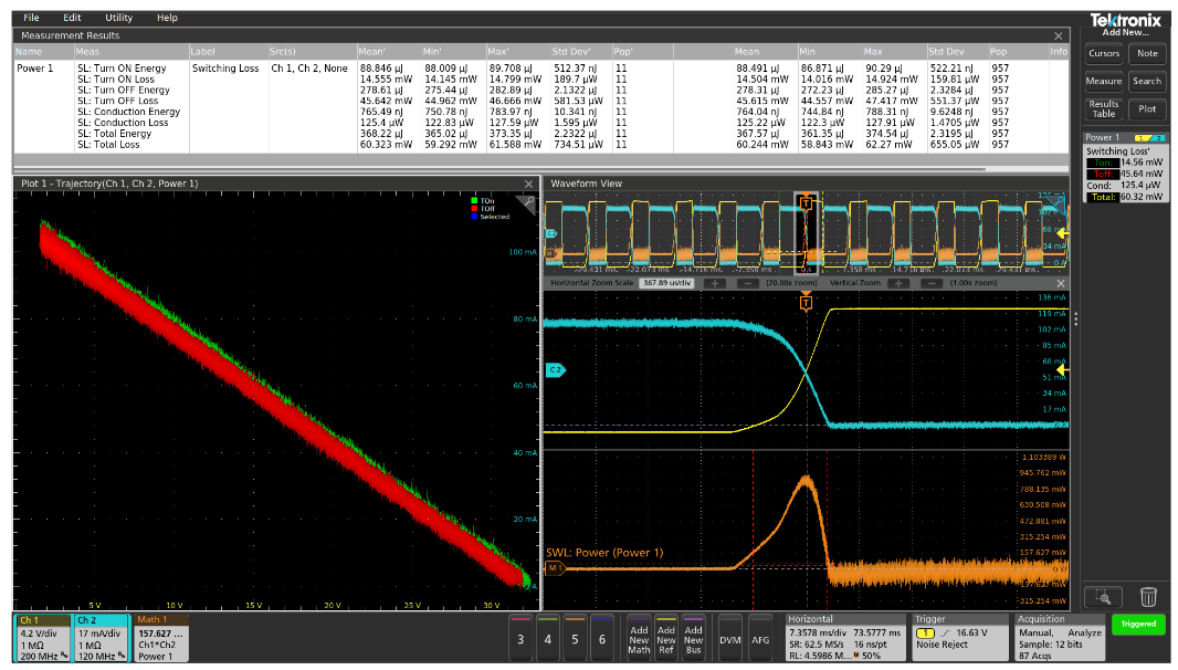
多くのオシロスコープは、自動測定を使用してこのプロセスを改善することができます。自動振幅と立ち上がり時間の測定を使用して信号の振幅を決定し、その振幅の10%と90%で測定閾値を設定し、信号の立ち上がり時間を測定することができます。さらに、複雑な信号の場合、カーソルゲーティングを使用して波形の特定の部分に焦点を当て測定することができます。その後、スルーレートは振幅を80%で乗算し、立ち上がり時間の測定値で割ることによって計算されます。

電力分析ソフトウェアを使用すると、スルーレート測定のセットアップが容易になり、回路内のコンポーネント値を設計エンジニアが調整する際の測定結果のばらつきを減少させられます。

LIV curves
図7. MOSFETゲート信号における自動スルーレート測定

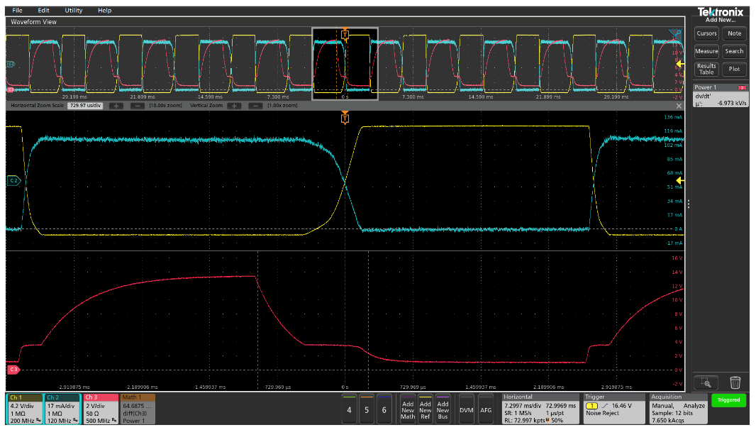
図7のチャネル3で赤色に示されているMOSFETゲート(VGS)におけるカーソルゲートされたスルーレート測定では、スイッチングデバイスのゲートに予想以上の容量があったため、スイッチング信号が設計仕様よりもはるかに遅かったことを示しています。

図7で垂直カーソル間に示されている指数関数的減衰は、ゲート駆動回路の出力インピーダンス、スイッチングMOSFETデバイス内の寄生ゲート容量、およびゲートにおける回路基板の容量の影響によるものです。ゲート駆動の出力インピーダンスを減少させ、ゲートノードの容量を低減させることにより、駆動信号の速度を高めたところ、図8に示されるように、スイッチング損失がほぼ30%改善されました。

LIV curves
図8. 自動スイッチング損失測定により、大幅な改善が示されています。

スイッチング損失測定は、スイッチモード電源の効率を最適化するための重要な部分です。良い測定技術を使用し、電力測定を自動化することで、複雑なスイッチング損失測定の一連を簡単に、迅速かつ繰り返し行うことが可能になります。

LIV curves LIV curves

tek.comでさらに価値あるリソースを見つけましょう。


Copyright © Tektronix. All rights reserved. Tektronix製品は、登録済みおよび出願中の米国その他の国の特許等により保護されています。本書の内容は、既に発行されている他の資料の内容に代わるものです。また、本製品の仕様および価格は、予告なく変更させていただく場合がございますので、予めご了承ください。TEKTRONIXおよびTEKは、Tektronix, Inc.の登録商標です。 その他、記載されているすべての商号は、それぞれの会社のサービスマーク、商標または登録商標です。

09/19 46W-60010-3


Switching Loss Measurements_App-Note_46W-60010-3

Measuring Power Supply Switching

Loss with an Oscilloscope

––

APPLICATION NOTE

Application Note

Line


Gate

Drain

Neutral

Source

Ground


Gate


Drive


Figure 1. Simplified switch mode power supply switching circuit.

Introduction

With the demand for improving power efficiency and extending the operating time of battery-powered devices, the ability to analyze power loss and optimize power supply efficiency is more critical than ever before. One of the key factors in efficiency is the loss in switching devices.

This application note will provide a quick overview of these measurements and some tips for making better, more repeatable measurements with oscilloscopes and probes.

A typical switch-mode power supply might have an efficiency of about 87%, meaning that 13% of the input power is dissipated within the power supply, mostly as waste heat.

Of this loss, a significant portion is dissipated in the switching devices, usually MOSFETs or IGBTs.

Ideally, the switching device is either “on” or “off” like a light switch, and instantaneously switches between these states. In the “on” state, the impedance of the switch is zero and no power is dissipated in the switch, no matter how much current is flowing through it. In the “off” state, the impedance of the switch is infinite and zero current is flowing, so no power is dissipated.

Measuring Power Supply Switching Loss with an Oscilloscope


Turn-on Turn-off


Region

Region


t0

t1

t2

t3


v(t)


off

on

off

on

0

i(t)


Switch Voltage and Current


p(t) = v(t) * i(t)


0


Switch Power Loss


A.

B.


How switch

How the

appears on

circuit sees

schematic

the switch

Figure 2. Multiplying instantaneous voltage across and current through a switching device gives instantaneous power throughout the switching cycle.

Figure 3. A: How the switch appears on the schematic, and B: How the circuit sees the switch.

In practice, some power is dissipated during the “on” (conduction) state, and, often, significantly more power is dissipated during the transitions between “on” and “off” (turn-off) and between “off” and “on” (turn-on).

These non-deal behaviors occur because of parasitic elements in the circuit. As shown in Figure 3b, the parasitic capacitances on the gate slow down the switching speed of the device, extending the turn-on and turn-off times. The parasitic resistances between the MOSFET drain and source dissipate power whenever drain current is flowing.

Application Note

Conduction Loss

In the conduction state, the switch does have a small resistance and voltage drop across it, and the switch dissipates power as a function of the current flowing through it.

For a MOSFET, this power is typically modeled as:

P = ID2 * RDSon = ID * VDS

-where ID is the Drain current,

-RDSon is the dynamic on-resistance between the Drain and the Source, often < 1 Ω, and

-VDS is the saturation voltage between the Drain and the Source, often < 1 V

For an IGBT or BJT, this power is typically modeled as:

P = IC * VCEsat

-where IC is the Collector current and

-VCEsat is the saturation voltage between the Collector and the Emitter, often < 1 V

Turn-on Loss

During turn-on, the current through the switch rapidly increases and the voltage drop across the device quickly decreases. However, parasitic elements, such as the Gate-to-Drain capacitance in a MOSFET, prevent the switch from turning on instantaneously. While the device is turning on, there is significant current flowing through the device and significant voltage across the device, and significant power loss occurs.

For a MOSFET, during turn-on, this power is typically modeled as:

P = ID * VDS

-where ID is the Drain current and

-VDS is the voltage between the Drain and the Source

For an IGBT or BJT, during turn-on, this power is typically modeled as:

P = IC * VCE

-where IC is the Collector current and

-VCE is the Collector to Emitter voltage

Turn-off Loss

In a similar manner, during turn-off, the current through the switch rapidly decreases and the voltage drop across the device quickly increases, but circuit parasitics prevent the switch from turning off instantaneously. While the device is turning off, there is significant current flowing through the device and significant voltage across the device, and significant power loss occurs. The equations above also apply.

Measuring Power Supply Switching Loss with an Oscilloscope

Measuring Switching Loss

There are two approaches to measuring switching loss: it can be measured using manual setups and built-in oscilloscope measurements, but there are also automated measurement systems available on some oscilloscopes. The automated measurements have the advantages of being easy to set up and delivering easily repeatable results. With either technique, careful probing and optimization will help you get good results.

Probing and Measurement Setup

Before discussing the specific power measurements, there are six key steps to making accurate and repeatable measurements:

1.Remove voltage offset errors: The amplifiers in differential probes may have a slight DC voltage offset which will affect measurement accuracy. With the inputs shorted and no signals applied, automatically or manually adjust the DC offsets in the probe to zero.

2.Remove current offset errors: Current probes may also exhibit DC offset errors due to residual magnetism in probe, as well as amplifier offsets. With the jaws closed and no signals applied, automatically or manually null out the DC offsets in the probe.

3.Remove timing errors: Because instantaneous power measurements are calculated based on multiple signals, it is important that the signals be properly time-aligned. Different technologies are used to measure voltages and currents, and the propagation delays through these devices

may be significantly different, leading to measurement errors. Good results are generally possible by adjusting the inter-channel timing to account for the difference in nominal propagation delays in the deskew menu. For the most accurate results, apply a high-slew-rate signal to all inputs and carefully remove any relative timing offset (skew) between all channels.

4.Optimizing Signal-to-Noise Ratio: In all measurement systems, but especially in digital devices such as modern oscilloscopes, good measurement technique requires keeping signals as large as possible (without clipping) to minimize the effects of noise and to maximize vertical resolution. This includes using the lowest necessary attenuation when probing the signals and using the full dynamic range of the oscilloscope.

5.Signal conditioning: Measurement quality can also be improved by conditioning the input signals. Bandwidth limiting can be used to selectively reduce noise above the frequencies of interest, and averaging can be used to reduce uncorrelated or random noise on the signal. High Res acquisition mode provides bandwidth limiting and noise reduction, increased vertical resolution, and it even works on signals acquired in single shot mode.

6.Accuracy and safety: For best accuracy, be sure to use the equipment within the normal operating range and below the peak ratings. And, for your safety, always stay well within the equipment’s absolute maximum specifications and follow manufacturer’s instructions for use.

Application Note

Figure 4. Switching power loss measurement using waveform multiplication and mean measurement on the power data over the whole acquisition. This technique relies on manual setup, using standard capabilities of this oscilloscope.

Measuring Switch Loss – Manual Setup and Built-in Measurements

One way to measure turn-off loss is with gated measurements. The object is to measure the average power dissipated during the turn-off phase. In this example, the MOSFET’s

VDS is acquired with a differential voltage probe and is shown in yellow in Figure 4. The Drain current is acquired with an AC/DC current probe and is shown in cyan. The vertical sensitivity and offset of each channel is adjusted so the signals occupy more than half of the vertical range, but without extending beyond the top and bottom of the graticule.

A stable display is important for visual analysis, so the oscilloscope’s edge trigger is set to the 50% point on the voltage waveform. Then the sample rate is set to assure adequate timing resolution on the signals’ edges. In this case, a sample rate of 6.25 GS/s results in many sample points on each edge of the switching waveform. Finally, High Res acquisition mode is enabled to increase the vertical resolution to 16 bits.

Waveform math is then used to multiply the current by the voltage to create the orange instantaneous power waveform. An automated measurement is used to measure the average or mean value of the power waveform.

In this example, the engineer manually adjusted the oscilloscope to optimize the quality of the switching loss measurement. At a later date, this engineer or another engineer would likely set up the measurement slightly differently, resulting in different measurement results. Automating the measurement through power analysis software removes many of the sources of variation.

Measuring Power Supply Switching Loss with an Oscilloscope

Figure 5. Automated switching loss measurement determines power and energy loss during turn-on, turn-off, and conduction. In this case the power analysis software automatically sets up the measurement when the Switching Loss measurement is turned on.

Measuring Switch Loss – Automated Using Power Analysis Software

To consistently optimize the setup and improve measurement repeatability, a power measurement application can be useful. In this case, the PWR Advanced Power Analysis application provides a custom autoset for the Switching Loss measurement and then, with the push of a button, makes the full suite of switching loss power and energy measurements.

Slew Rate and Switching Loss

As expected from inspecting the instantaneous power waveform and as indicated by the switching loss measurement values in Figure 5, the turn-off loss is the dominant loss mechanism in the total switching loss. A potential cause of this high loss is the performance of the switch drive circuit. If the transition time or slew rate of the drive signal is slower than expected, the switch will remain between on and off states longer than expected, and the switching losses will be higher than expected.

Application Note

Figure 6. A trajectory plot shows voltage versus current during turn-on (green traces) and turn-off (red traces) over many cycles, showing how switching changes over time. In this test circuit the drain current is limited by resistors, so the plots are linear.

A slew rate measurement is the change of voltage in a given time interval (usually between the 10% and 90% points on an edge) and has the units of volts/second. Because the mathematical derivative is inherently a high-pass filter, and thus will accentuate noise, it is recommended that you use averaging to reduce the effects of random noise on these measurements.

Slew rate measurements can be made manually with cursors by placing one waveform cursor at the 10% point of the signal edge and the other cursor at the 90% of the waveform edge.

The slew rate is then calculated by dividing the difference between the voltage measurements by the time difference between the cursors. This technique requires the user to estimate the 10% and 90% points on the waveform and calculate the result.

Measuring Power Supply Switching Loss with an Oscilloscope

Figure 7. Automated slew rate measurement on a MOSFET gate signal.

Many oscilloscopes can improve this process with automatic measurements. Automated amplitude and rise-time measurements can be used to determine the amplitude of the signal, set the measurement threshold values at 10% and 90% of that amplitude, and then measure the rise-time of the signal. And, in the case of a complex signal, cursor gating can be used to focus the measurement on a specific portion of the waveform. Then the slew rate is then calculated by multiplying the amplitude by 80% and dividing by the rise-time measurement.

However, power analysis software makes slew rate measure- ment setup easy, and it reduces variation in measurement results as the design engineer adjusts component values in the circuit.

A cursor-gated slew rate measurement on the MOSFET gate (VGS, shown in red on channel 3 in Figure 7) shows that the switching signal was much slower than the design spec, because of higher-than-expected capacitance at the gate of the switching device.

Application Note

Figure 8. Automated switching loss measurement, showing significant improvement.

The exponential decay, shown between the vertical cursors in Figure 7, is a function of the output impedance of the gate drive circuit, the parasitic gate capacitances within the switching MOSFET device, and the circuit board capacitances at the gate. When the speed of the drive signal was increased, by reducing the gate drive output impedance and the capacitance at the gate node, the switching loss was improved by almost 30%, as shown in Figure 8.

Switching loss measurements are a critical part of optimizing the efficiency of switch mode power supplies. By using good measurement techniques and automating the power measurements, it is easy make a series of complex switching loss measurements, quickly and repeatably.

Measuring Power Supply Switching Loss with an Oscilloscope

Several Tektronix oscilloscope series offer automated switching loss measurements. Consult www.TEK.COM for information on specific instruments. The measurements shown in this application note were made with the following equipment:

5 Series MSO

5-PWR Advanced Power

Analysis Application

TDP1000 1 GHz Differential Probe

TCP0030A 120 MHz AC/DC Current Probe

www.tektronix.com/power-supply-measurement-and-analysis 11

Copyright © Tektronix. All rights reserved. Tektronix products are covered by U.S. and foreign patents, issued and pending. Information in this publication supersedes that in all previously published material. Specification and price change privileges reserved. TEKTRONIX and TEK are registered trademarks of Tektronix, Inc. All other trade names referenced are the service marks, trademarks or registered trademarks of their respective companies.

09/19 EA 46W-60010-3