Abstract
Clock recovery is a common part of many measurements, whether as part of the test setup or part of the device under test. We’re going to look at clock recovery from a practical point of view, with emphasis on how it affects measure-ments. This document closely mirrors the poster "The Anatomy of Clock Recovery, Part 2" and picks up where the paper "Clock Recovery Primer, Part 1," left off.
9. Loop Types and Orders
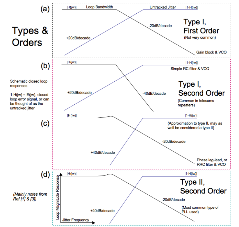
Phase lock loops in systems are often complex, and based on digital architectures that are impossible to model. However, standards tend to use simpler analog PLLs as models to communicate the behavior expected. A very high level summary of types and orders follows. Much more detail can be found in references [1], [2], and [3].
Notes on Type II Loops[1]
Second Order, Type II (SOTII)
- The vast majority of clock recovery loops are either based on SOTII loops, or are designed to be approximately second order.
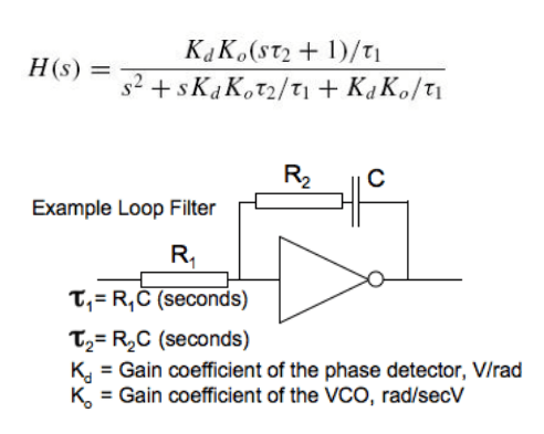
- The mathematical expression of the transfer function can be of the form shown in the section below. The order is taken from the highest power of 's' in the denominator (second order, as s2 in the equation)
- Many of the important properties of loop behavior relate to the Type of the loop, rather than the order.
- The type refers to the number of pure integrators in the loop.
- The VCO itself has an integrating effect. A Type II loop as discussed in this section is one with a perfect integrator in its loop filter in addition to the VCO.
- The Order can never be less than the Type.
- A loop can have other, non-integrating filtering in the loop, which does not affect the Type but can increase the Order.
- SOTII are unconditionally stable for all values of loop gain.
- Damping factor ζ (zeta) only applies to second order loops.
- All SOTII loops have some degree of peaking, even for very highly damped systems.
- Peaking of less than 0.1 dB requires a damping factor of >4.4
- Damping factors less than 0.5 have excessive overshoot in their transient responses.
- SOTII H(jω) asymptotically rolls off at –6 dB/octave (–20 dB/decade)
- Different slopes are produced for PLLs of different Orders.
- SOTII Error (1 – H(jω)) asymptotically rises at +12 dB/octave (+40 dB/decade)
- Different slopes are produced for PLLs of different Types
Example SOTII Transfer Function
s = σ + jω Transform complex variable of a Laplace transform (Tutorial in Appendix B of Reference [2])
H(s)= closed loop transfer function
Notes on Type I Loops[1]
- Varieties:
- Can be a VCO on its own (single integrator) with just a gain block between phase detector and VCO (First Order)
- Can be a VCO and a loop filter that is not a perfect integrator (Second Order, Type I). This variety is often used in telecom repeater applications.
- It is difficult to go back in history to the formation of many standards, but it is likely that when 'Type I' is specified in a standard, a Type I Second Order with a simple single pole filter is being referred to ((diagram b) in the following graphs).
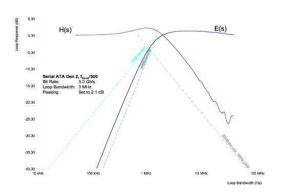
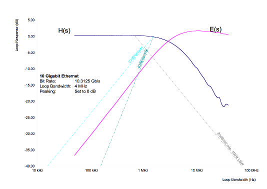
Notes on Responses
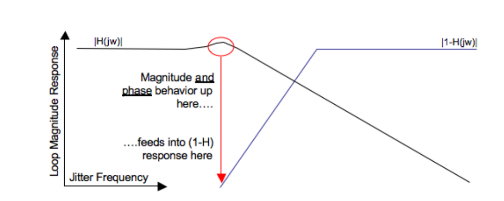
- The transfer response, H(s) shows the jitter the loop tracks. E(s) shows the jitter the loop does not track. H(s) and E(s) are complex quantities. E(s) = 1 - H(s).
- Conceptually, E(s) shows the amount H(s) deviates from 1, or the 0 dB line on the graph. This is a crude approximation to aid understanding — the true result involves both phase and magnitude in the calculation. For example, peaking may be present in one amplitude response that may not be present in the other.
- The graphs in Figure 20 show magnitude information only
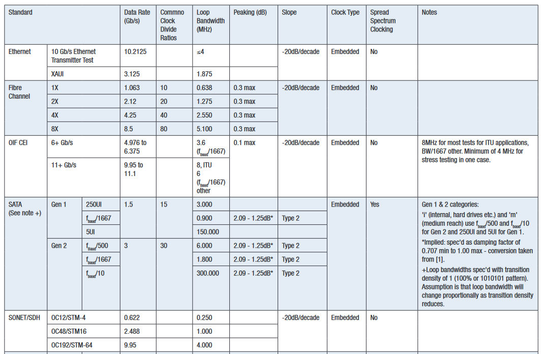
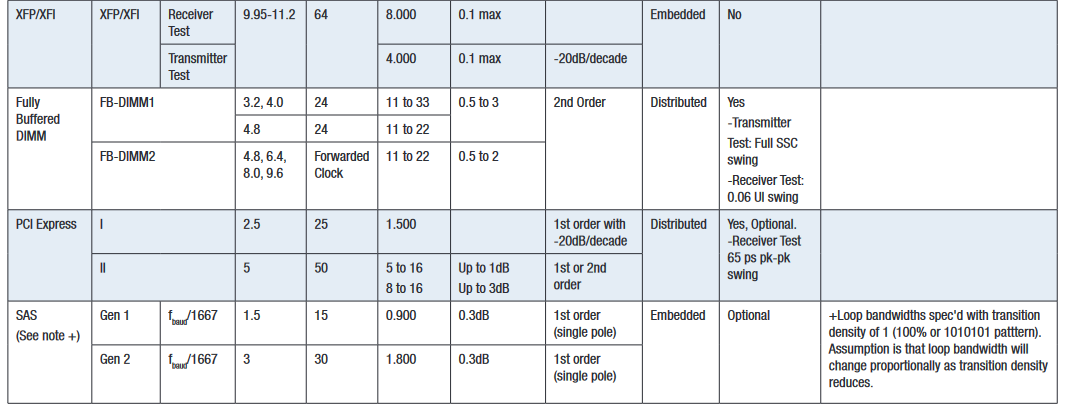
10. Survey of Clock Recovery Used in Selected Standards
Note: Standards are often ambiguous and open to interpretation. This summary is not a substitute for time taken reading and understanding the original document, including footnotes.
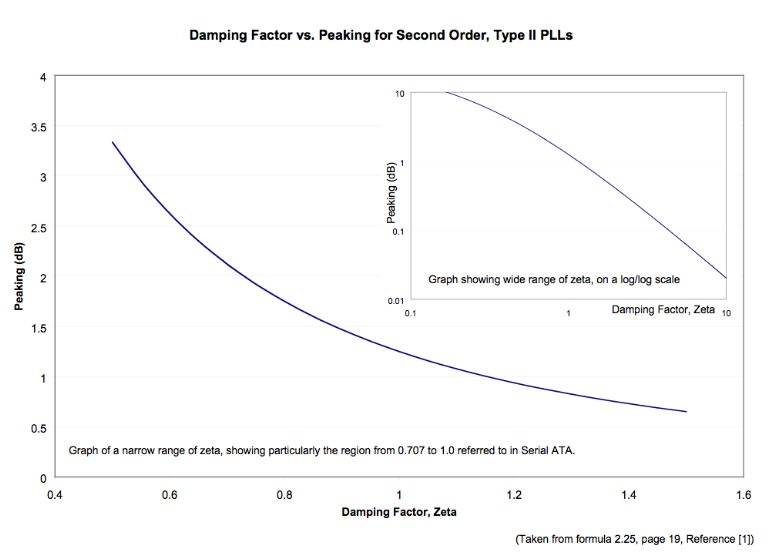
Note that Serial ATA specifies the peaking in terms of a damping factor range. Figure 22 shows a plot of how damping factor and peaking relate to each other.
Note that Serial ATA specifies the peaking in terms of a damping factor range. Figure 22 shows a plot of how damping factor and peaking relate to each other.
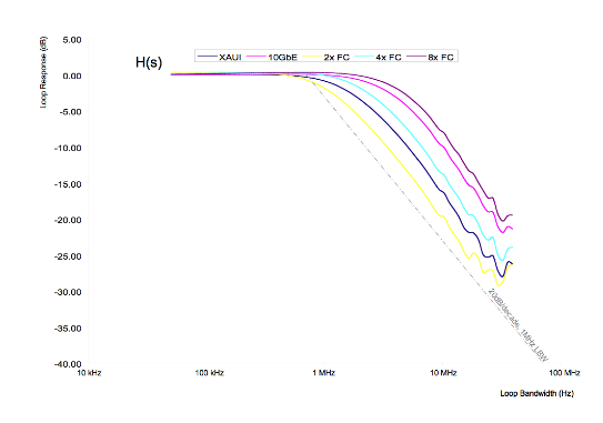
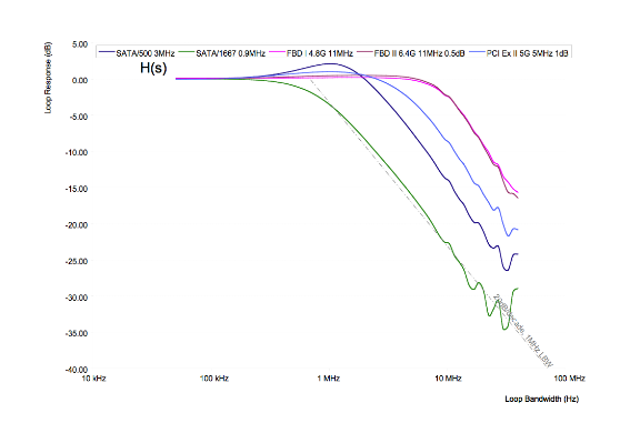
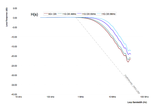
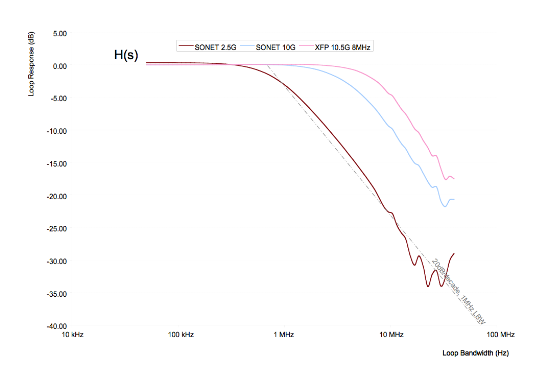
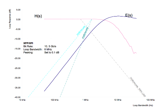
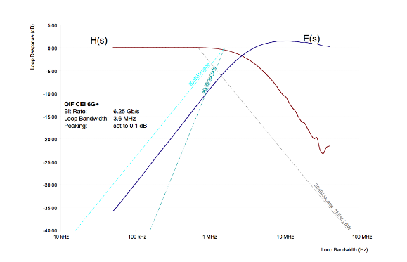
Example Measured Loop Responses Suitable for Different Standards
The graphs in Figures 23 through 30 show some measured example responses for different standards.
Notes:
- Ripple at high loop bandwidths in these graphs is a feature of the measurement system rather than the loop.
- The reference (dotted) lines are placed in identical positions in each graph to aid comparison.
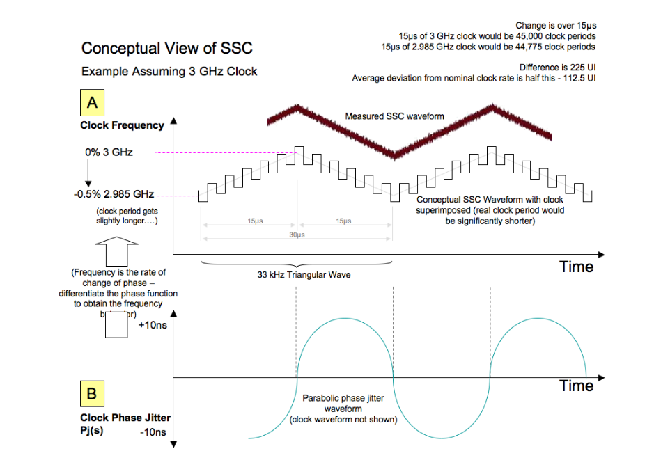
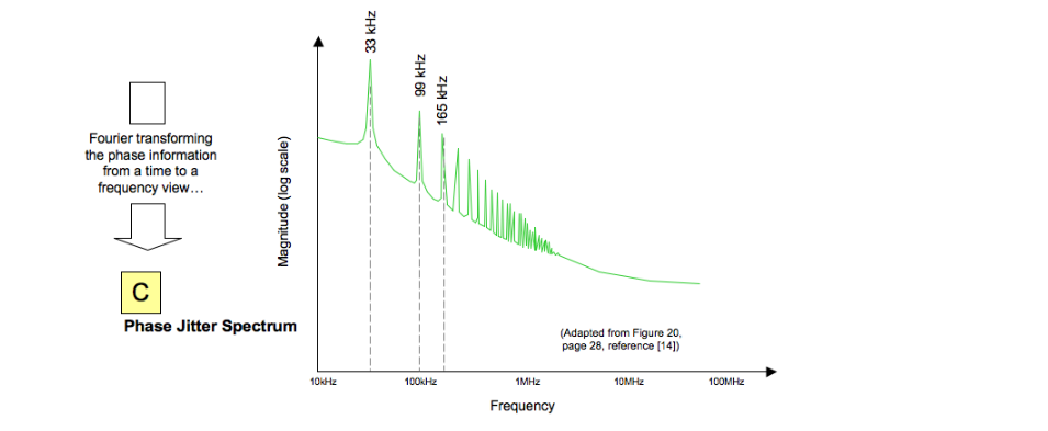
11. Spread Spectrum Clocking
Spread Spectrum Clocking is a requirement in Jedec’s Fully Buffered DIMM and SATA-IO’s Serial-ATA. It is an optional part of PCI Express, and Serial Attached SCSI (SAS). The aim is to spread the energy of the clock (and therefore data) over 0.5% of the frequency band, so the average power at a given frequency in the spectrum becomes lower. This helps products to comply with regulatory requirements for radiated and conducted emissions.
The standards listed above have the same specification requirement: Movement from +0% to -0.5% of the nominal data rate frequency. The modulation rate should be in the range not exceeding 30 kHz to 33 kHz. The data rate frequency excursion is also sometimes referred to in parts per million (ppm). The -0.5% excursion above equates to a -5000 ppm downward modulation. Sometimes lower excursions are employed, for example -3000 ppm. The exact waveform shape is not specified, but commonly is triangular in the frequency domain, parabolic in the phase domain.
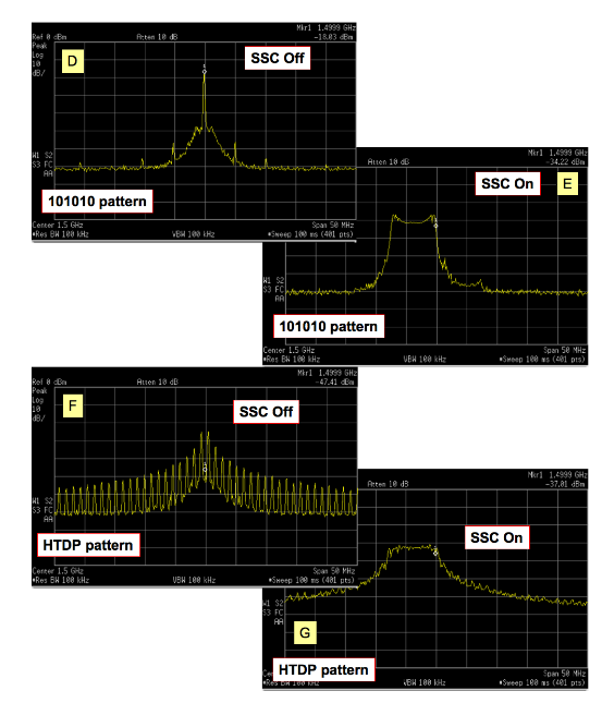
A, B and C are three schematic views of Spread Spectrum Clocking. The phase detector in clock recovery responds to changes in phase, making B and C the most appropriate to visualize how it reacts to an SSC signal. For most engineers, the frequency domain is an easier place to start than the phase domain, and measurements D/E and F/G may be helpful.
Frequency Domain View of SSC
A 101010 pattern viewed with SSC switched off (D) and on (E) is shown (Figure 32 upper). The ~12 dB reduction in average power is the reason why this form of modulation is popular in reducing measured electromagnetic emissions (EMI) in equipment. Note that it is only the measured (average) power that is reduced — the instantaneous power is the same in both cases. Measurements F and G are the same setup but with the pattern changed from 101010 to a valid Serial ATA test pattern, HTDP (High Transition Density Test Pattern).
SSC and Clock Recovery
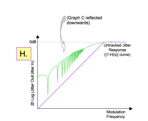
For a receiver to successfully track out SSC, it must be able to track the modulation, including its harmonics. The lower diagram (H) shows the loop error response (not to scale) with the SSC phase spectrum reflected down onto it. The loop must track the modulation sufficiently that significant eye closure does not occur. This is a situation where trigger delay is particularly important, as it could easily lead to a closed eye. See Section 13 of the poster, "Anatomy of Clock Recovery, Part 2."
Example Measurements (1)
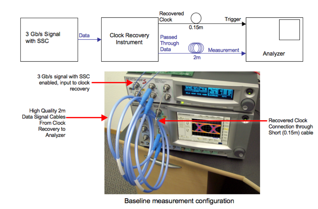
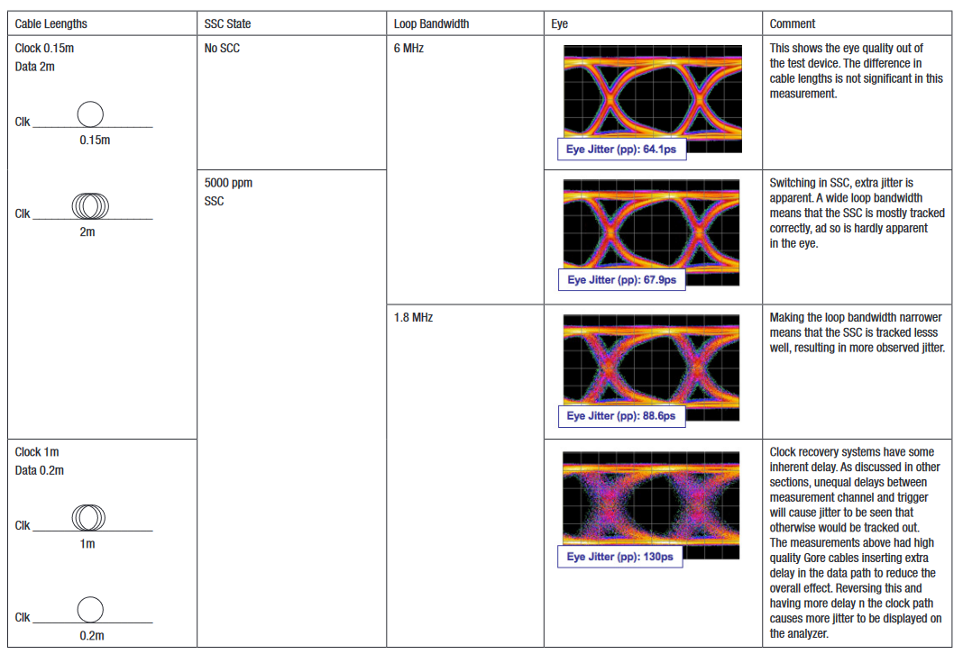
A 3 Gb/s signal with and without SSC was measured using a clock recovery instrument and an analyzer. Here we are going to look at the effect of loop bandwidth and cable delay on eye measurements. Data paths were differential.
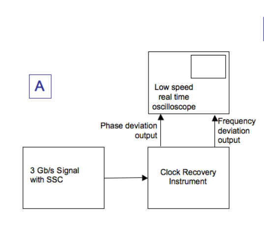
Example Measurements (2)
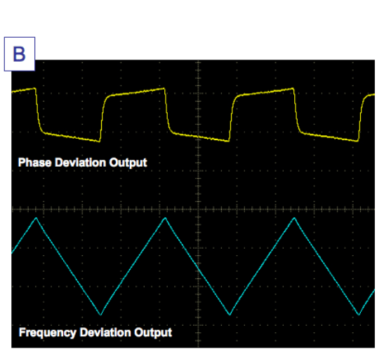
In this example, a signal with SSC was measured with a clock recovery instrument (A). Outputs on the rear panel of the instrument provide monitoring points to view the loop behavior. When viewed on a low bandwidth, real time oscilloscope, the traces in B were obtained. The triangular waveform characteristic of the common form of SSC is clearly visible in the lower trace. The yellow waveform displays the difference in phase between data input and clock recovery output; shown is the response to a ramp in frequency, first positive then negative, as expected from a second order Type 2 PLL setting.
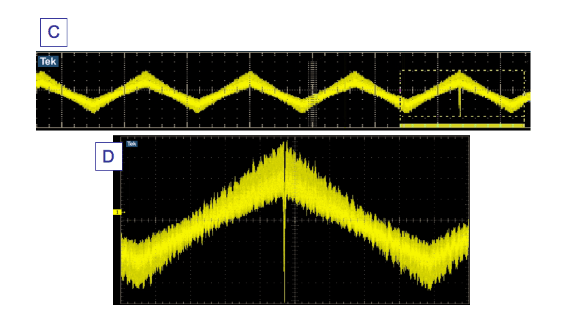
A similar setup was used to measure the output of a Serial ATA disk drive purchased in a local store. As can be seen in a captured waveform of C, and magnified in D, an abnormality is clearly visible with the drive. A glitch is occurring approximately every 100 periods or so. Although this glitch is within the allowed deviation for a SSC signal, it would be very likely to cause higher than expected jitter in the data waveform, resulting in poorer BER performance for the drive.
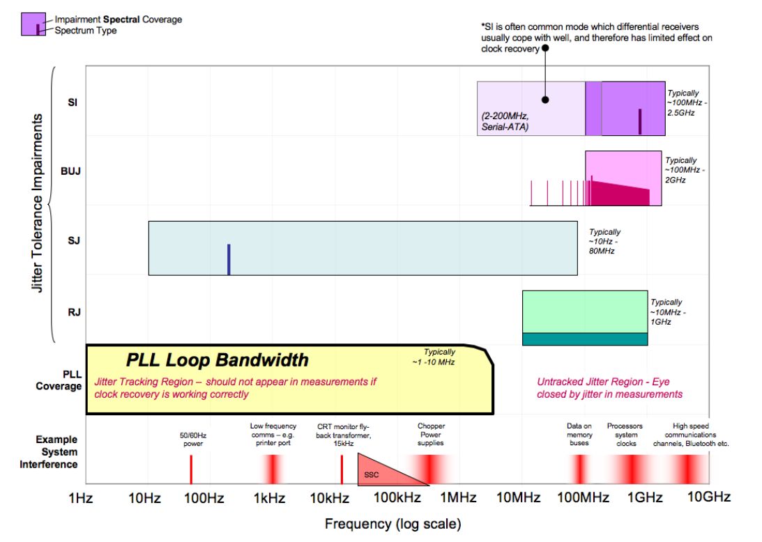
12. Testing Clock Recovery Using Stress
Figure 38 maps loop bandwidth alongside some common stress testing impairment types. It also shows some impairments that are often present in a real system. Inter Symbol Interference (ISI) is not shown. Arising from bandwidth limitations often present in channels, it is considered high frequency Data Dependent Jitter, and its interaction with clock recovery can be subtle.
Jitter Tolerance Testing and Loop Response
One element of receiver jitter tolerance testing in most standards is the application of sinusoidal jitter (SJ) of different frequencies and magnitudes. This is usually to a template such as (1) in Figure 39, where many unit intervals of jitter are applied at low frequency, and at high frequency a lower amount usually less than half a unit interval (UI).
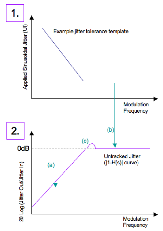
The lower graph shows the loop’s error response the jitter that is not tracked. In the lower frequency region (a), as long as the applied jitter magnitude at a given frequency is sufficiently tracked by the loop response, then no serious eye closure will occur. At high frequency, there is essentially no jitter tracking (b). The position of the knee in either curve relative to the other is obviously critical. So is the slope of the error curve, and any peaking that may be present (c).
BUJ Testing and Clock Recovery
Bounded Uncorrelated Jitter (BUJ) is a type of jitter modulation used in standards such as OIF CEI[6], and optionally Fibre Channel[5]. It involves modulating clock and data edges with a band-limited PRBS signal. It is intended to emulate effects such as interference and crosstalk in the system. One of the aims in a test environment is to introduce well controlled impairments with predictable effects. As can be seen in the stress table, most stress impairment types either operate above the tracking region of clock recovery, or are used to deliberately probe clock recovery (SJ). BUJ is in a grey area, where it can have some subtle interactions with clock recovery.
The BUJ graphic in the stress table assumes a 2 Gb/s PRBS-7 modulation. The lower end of the spectrum is around 15 MHz, above the loop bandwidth. As described in some standards, such as OIF CEI, BUJ is aggressively low pass filtered at between 1/10th and 1/20th of the modulation data rate, and has additional wider band low pass filtering approaching the modulation rate. The aim is to keep the distribution well controlled and bounded. A short PRBS pattern at a high modulation rate is fairly benign.
To show how the situation gets more complex, this discussion uses simulations of a low pass filtered 10 Gb/s PRBS-15 modulation. Figure 41 shows a section of the 32,767-bit pattern, displayed as edge deviations from positions they would have if they were unjittered (0 on the graph). The same data is also plotted as a Probability Density Function (PDF) on the right hand side.
The first graph shows a typical BUJ modulation behavior coming from the hypothetical pattern generator. The over filtering of the BUJ modulation pattern causes the edge deviations shown. The PDF has the intended sharp roll off shoulders and a well behaved, bounded distribution.
Passage of the signal through clock recovery has the effect of tracking low frequency jitter, and not tracking high frequency jitter. When the recovered clock signal is compared with the jittered data signal at a receiver or test analyzer, low frequency components are tracked, and net out. High frequency components of the jitter do not. The net effect is a high pass filtering of the jitter. For signals with appreciable spectral components below the loop bandwidth of the clock recovery in use, the effect is very like baseline wander. This can be clearly seen in graph 2, comparing the signal to dotted reference lines 'b,' and then the same for Graph 1 and dotted lines 'a.' The result is tails appearing in the PDF (well behaved and bounded in 'c', low probability tails visible in 'd'). When such a result is convolved with real world random jitter, the result can be infrequently occurring events that cause repeatability issues in measurements.
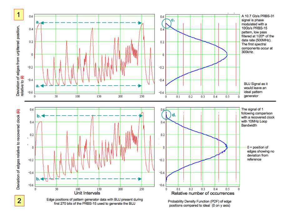
These effects arise when there is significant energy inside the loop bandwidth. The example, using a BUJ modulation of PRBS 15 at 10 Gb/s, has modulation spectral components starting at 300 kHz, well inside the loop bandwidth of the clock recovery used. BUJ modulation with longer patterns (for example, PRBS 31) would make this effect considerably worse, as would use of low modulation rates such as 100 Mb/s. Shorter patterns repeat frequently and do not have long tails, so have less effect even at low modulation rates.
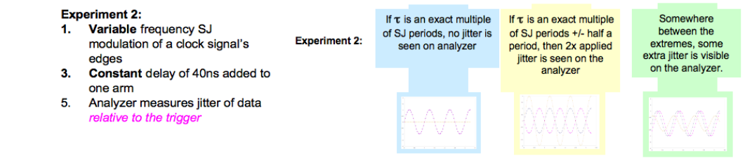
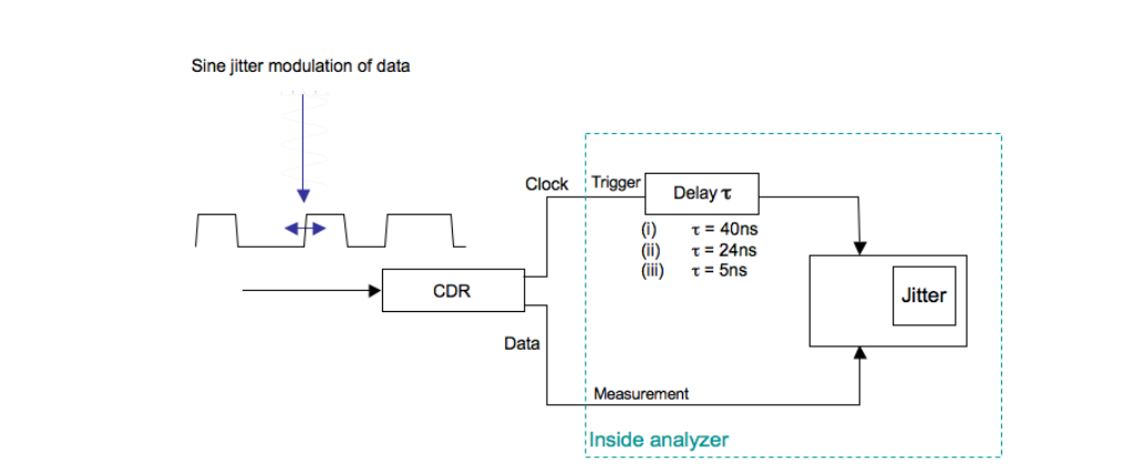
13. The Effect of Trigger Delay in Measurements
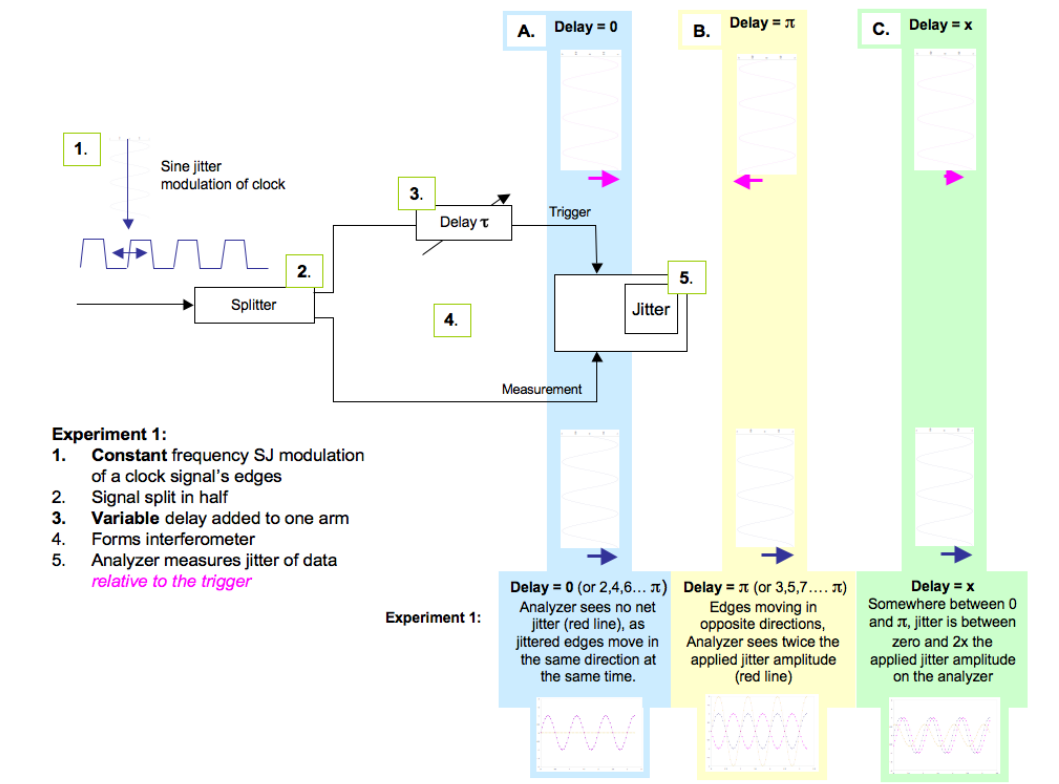
Imagine an experiment set up as shown in Figure 42. We will use this to show the effect of Trigger Delay
Conclusions:
- A fixed delay in the measurement system could cause additional apparent jitter to be measured.
- The additional jitter magnitude is dependent upon the jitter frequency relative to the amount of delay.
Practical Consequences
Most test equipment has a delay on the trigger path relative to the measurement path inside the analyzer. The effect can become visible when measuring clock recovery circuits, as we’ll see. First, let’s look at how the delay effect behaves.
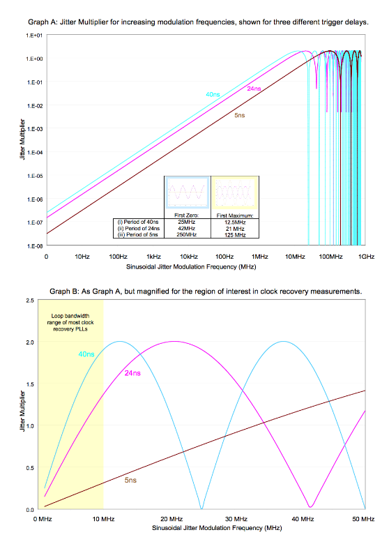
At low modulation frequencies, the delay difference is small compared to the period of the modulation. As the frequency increases, the delay becomes a more significant percentage of the period, and the equipment induced jitter becomes larger, until it peaks by effectively doubling the measured jitter. The overall effect is shown in Graph A over many modulation frequency decades. The scale is logarithmic in frequency. Because the interferometric effect is sinusoidal, it periodically dips to zero (as discussed above). Graph B is a magnified version, showing the area relevant to typical CDR measurements. In these graphs, cases are shown for equipment delays of 5, 24, and 40 ns. These equate to the BERTScope intrinsic delay, and two delays associated with sampling oscilloscopes, respectively.
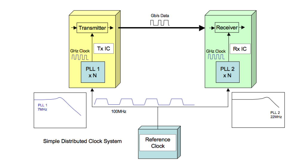
14. Clock Scheme Notes (1): Distributed
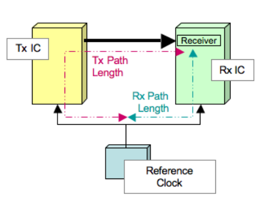
Up to now, we have primarily looked at systems where the clock is derived from the data stream. PCI Express[12] and Fully Buffered DIMM[11] are two systems where the architecture uses a distributed clock routed to each end of the communication link to time data. PLLs are used on the transmit and receive ends to multiply up the reference clock, and some behaviors unique to distributed systems are discussed here. Significantly more rigor can be found in Reference [14].
A lower frequency reference clock is distributed to each IC in this example at 100 MHz. This reference clock will have jitter on it, for example from the phase noise of the originating crystal. It might also have Spread Spectrum Clocking (SSC). The clock is multiplied up within each IC, and used to clock transmit and receive functions. Each PLL will have a loop response, and providing PLL 1 and 2 have identical behavior, jitter on one should be tracked exactly by the other, such that the receiver sees no net effect. Reality tends to be more complex.
Even for devices manufactured with the same design, fabrication process, and manufacturing lot, it is virtually impossible to get identical loop responses. It is also difficult to ensure identical path lengths between and within ICs, so the equivalent of the trigger delay discussed earlier can be an issue. We’re going to look at how the jitter is affected through the system.

Modeling of the effect of two different PLL responses combined is shown in the graph. Each individual PLL needs to track the reference clock jitter, and the difference in the way they track determines the system’s reference clock jitter rejection. The effect at the receiver depends on not only the loop bandwidths, but also whether the higher of the two loop bandwidths is located at the receiver or transmitter end. The difference between the two loop bandwidth locations is significant in the amount of jitter tracking, or jitter rejection, obtained.
As mentioned above, if clock path lengths are unequal in the system, then an equivalent of the trigger delay will be apparent in the receiver jitter. This has the effect of moving the combined response graph up, increasing the jitter seen by the receiver. For PCI Express, the path length mismatch is limited to a maximum of 30 ns.
15. Clock Scheme Notes (2): Clock Domains in Embedded Clock Systems
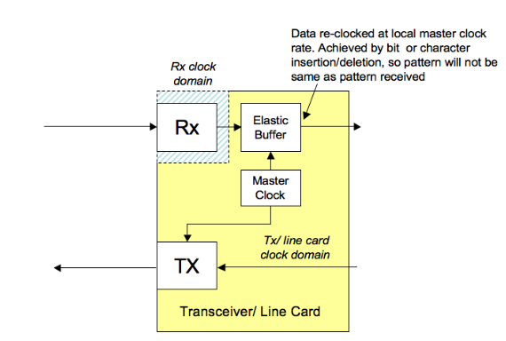
Embedding the clock into data is a common method of ensuring that accurate recovery of the transmitted data stream is achieved at the receiver. Once achieved, however, there is the problem of having a system running at one clock rate, and an incoming bit stream running at a slightly different rate. Somehow the data must be reclocked to match the receiveend system. In some architectures, such as SONET/SDH, a large amount of effort is made to try to keep all clocks in the system as closely matched as possible. This is achieved by distributing a highly accurate system clock based on GPS (Global Positioning Satellite), or local clocks based on Rubidium or similar standards. Other architectures assume more dissimilarity in clock rates to keep costs and complexity down. In either case, eventually the system must deal with the mismatch. Usually this is done by waiting until the difference becomes more than one bit, or one frame, and then inserting or deleting bits or characters. Often the system protocol will insert characters (or ‘fill words’) that can be sacrificed at the receiver, or the protocol will allow the receiver to insert ones of its own, if required, without disturbing the meaning of the data.
Impact on Test
Protocol based test equipment is usually set up to deal with inserted or deleted characters, and is able to recognize the underlying information. Physical layer test equipment is sometimes more limited, requiring patterns to conform exactly to an unchanging, known sequence that repeats. Extra or missing bits can throw the whole process off, causing the equipment to think errors have occurred.
A similar effect can occur in a system’s management of baseline wander that is, the way a system can be thrown off by AC coupling and long runs of identical bits, causing the average signal voltage to drift until bit errors occur. In this case, protocol schemes often have two versions of each valid character, and will decide to send the one that most effectively counteracts any baseline wander (‘running disparity’). The protocol intelligence at the receiver has no problem with recognizing either version as being correct, but again, this violates the need for an unchanging bit pattern in some test equipment.
In some test scenarios, it is possible to place the system in a test mode where a known pattern is sent or received, for example a PRBS-7, and protocol functions disabled. This makes physical layer testing easier, but is not always possible. This can be the case for operating network systems where the protocol cannot be turned off, or some transceivers in loop back mode.
Some test equipment can make some parametric measurements without the need for repeating patterns (sometimes called ‘Live Data Options’ or equivalent, on BERT equipment). This can be very effective at examining physical layer problems, but will be blind to protocol mistakes and bit errors that occur in a receiver but are cleaned up and resent by a transmitter as bits that are healthy, but wrong.
Loop Back Testing
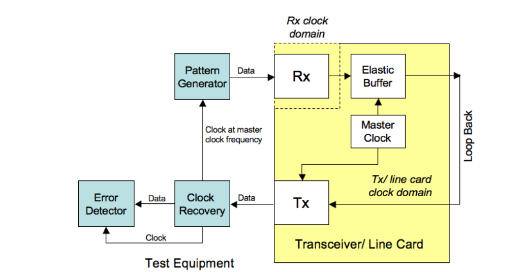
Often it is possible to perform loop back testing so that a signal sent into a receiver is looped back to become the output of the transmitter (Figure 49). It does not always follow that the data will be identical, however. As mentioned above, mismatches in clock rate can still cause fill word changes that might upset test equipment. A possible test scenario to get around this is shown below. The aim is to create a situation where the transmitter and receiver clock domains are absolutely identical, negating the need for domain rate matching.
- Recovering clock from the line card creates a clock at an identical frequency to the master reference to which the incoming data will be compared.
- Clocking the pattern generator with this ensures that the elastic buffer has no necessity to insert or delete fill words or bits.
- Error Detector pattern should be the same as the pattern sent out by the Pattern Generator.
- This is most likely to be successful if loop back is implemented as close to the transmitter and receiver blocks as possible, to avoid possibilities of logical (protocol) or SONET system errors being introduced from faults that fall outside the scope of parametric testing, or overhead changes such as readdressing being imposed.
Many standards, such as Ethernet and Fibre Channel, use the same coding schemes (known as 8B/10B), and have standardized test patterns described in MJSQ[15]. Patterns with names beginning with 'C,' such as CJTPAT and CRPAT, are termed 'compliant' in that they form valid frames that should fool equipment under test.
Summary
We have seen that clock recovery is increasingly common in systems and test setups. It can be a mistake to assume that you are ‘just deriving a trigger,’ for example, without considering the effect that trigger signal might be having on the measurement.
The two Clock Recovery Primer documents have covered considerable ground in the arena of clock recovery. It has been surprising how complex some of the topics explored turned out to be. The reader is encouraged to consult the references for detailed information, as most topics have been dealt with at a conceptual, shallow level only.