
Introduction
Timing jitter is a pervasive problem in the design of high-speed serial communication systems. If your job involves characterizing jitter, you will probably find that you need a clock or data source with intentional, controllable jitter from time to time. Depending on your objective, proper attention to detail in such a jitter source may be critical to obtaining reliable, repeatable results. Verification of the final jittered source with available measurement tools ensures generation accuracy
TDSJIT3 v2.0 is a software application that runs on Tektronix high-performance real-time oscilloscopes and provides a large suite of tools for jitter and timing analysis and visualization. When combined with the proper jitter sources, it is a powerful tool for verifying and analyzing jitter tolerance and jitter transfer characteristics.
Section 1 of this note explores how (and how not) to generate controlled jitter.
Section 2 reviews a few cases where you might use a jittered source, such as:
- Jitter Tolerance testing
- Jitter Transfer testing
- Test Equipment Correlation
This section also covers which aspects of jitter generation might require extra attention in each case, and suggests how TDSJIT3 v2.0 can be used to support the tests.
Section 1: Jitter Generation Techniques and Pitfalls
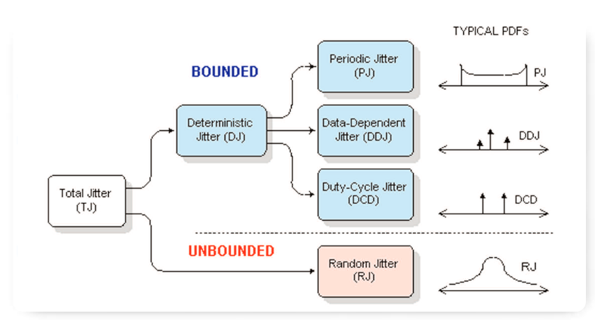
Timing jitter can be subdivided into various categories, such as random, data-dependent or (uncorrelated) periodic. These are commonly organized into a jitter hierarchy, as shown in Figure 1. You may have a need to generate one specific type of jitter, or a composite of two or more types. To be successful, you should understand
- What kind of jitter-generation tools might be at your disposal;
- What performance limitations each tool has; and
- How you can successfully combine the tools to achieve your goal.
Armed with this knowledge, you can efficiently create a test signal adequate for your specific task. Without it, you are likely to fall into one of the several traps that await the unwary.
1.1 Composite Jitter
If you need a jittered signal with a combination of jitter types (random, sinusoidal, DDJ, etc), an arbitrary waveform generator (AWG) is conceptually simple and easy is to use. The typical AWG can be thought of as a large memory buffer connected to a digital-toanalog converter, frequently though a programmable state machine that allows segments of waveform memory to be stitched together to create a complex pattern.
An AWG has several attributes that make it attractive. It can generate many different signal types: clock-like signals as well as data signals with almost any imaginable data pattern. The risetime and overshoot can be controlled with great precision (making it easy to create a wide variety of DDJ). An approximation of random jitter can also be included, and all these jitter types can be conveniently combined so that the output of the AWG provides everything required for the test.
However, the limitations of this approach should be clearly understood. Perhaps the biggest limitation is the quality of random jitter that can be produced. Since the data pattern from most AWGs is constrained to be periodically repeating (albeit perhaps with a very long period), the jitter is at best pseudo-random rather than truly random. Although the jitter so produced may look random to the eye, the probability distribution isn't suitable for any demanding applications. This topic is covered in greater detail in Section 1.2.
Periodic jitter can be modeled with an AWG but there are some limitations. The pattern length must be long enough to contain an integral number of cycles of the periodic jitter modulation, in order ensure that no discontinuity occurs when the pattern is repeated. If you want to create periodic jitter with more than one periodic component, the rule mentioned above must be satisfied for each component, enforcing a specific harmonic relationship between the components. And if the signal being modulated is a data signal rather than a clock signal, the data pattern length adds additional requirements to avoid discontinuity
A fundamentally different approach to creating composite jitter is to create the various jitter components separately and then combine them together. This approach is covered separately in Section 1.5.
1.2 Random Jitter
When it comes to serial communications testing, random jitter is universally defined to mean jitter with a Gaussian probability density function. This is often assumed to mean white Gaussian noise, where "white" means that the noise has equal power per decade when viewed in the frequency domain. Gaussian noise in communication links usually is white at higher frequencies, although it often exhibits other asymptotic tendencies (e.g. 1/f or 1/f2) at low frequencies. It is important to note that Gaussian noise isn't necessarily white, nor is white noise necessarily Gaussian.
A common approach to generating Gaussian voltage noise (which is later converted to timing jitter) is to use an instrument known as a noise generator. There is at least one well-known manufacturer that has made their name in noise generation. Use of an instrument of this kind can be acceptable even for demanding applications, but only if the instrument model is carefully chosen and provides adequate performance.
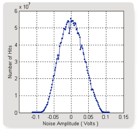
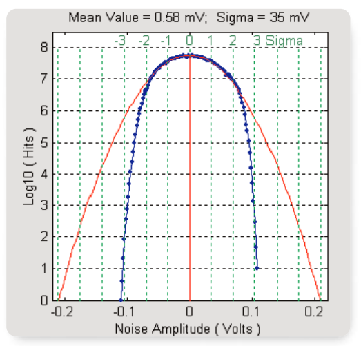
The key pitfall here is that a Gaussian voltage distribution theoretically has unbounded amplitude peaks, whereas in real instruments the output voltage is inevitably bounded by the power supply rails. The resulting truncation of the voltage distribution can occur at surprisingly low levels, in which case the noise generator will not be suitable for many tests. Figure 2a shows a histogram of voltage distribution from a general-purpose noise generator, collected over a several minute period and displayed on a linear scale in blue. To the eye, this distribution looks quite Gaussian. However, the same data is shown in Figure 2b using a logarithmic vertical scale, overlaid with a mathematically generated true Gaussian curve (red). Here it becomes obvious that the noise generator departs from the Gaussian curve roughly two standard deviations on either side of the mean.
To avoid this problem, the key specification that you must check is the crest factor of the noise generator, defined as the ratio of the peak voltage to the RMS voltage at the output of the instrument. If the crest factor is inadequate, you will get a truncated Gaussian distribution that diverges significantly from the actual statistics of noise in a communications link.
Communications links commonly use a BER of 10-12 as their specification point for eye closure. This BER corresponds to a crest factor of 7.03, or 16.9 dB. If your noise generator doesn't explicitly specify a crest factor that comfortably exceeds this level (or otherwise specify when voltage compression may occur), then you should assume that the noise is not adequately Gaussian for demanding applications. If you have a noise source but aren't sure whether it is sufficiently Gaussian, a method is given in Appendix A for evaluating the source, using a high-performance oscilloscope and a MATLAB script.
Once you have a Gaussian voltage waveform, it must be converted into timing jitter. This task is considered in Section 1.5.
1.3 Periodic Jitter
The simplest way to produce PJ (periodic jitter) is to use a signal generator that has an internal sine wave oscillator and an FM (or PM) modulator. This approach is usually limited to cases where you only need a single-frequency periodic modulation. If you want to generate PJ with two or more uncorrelated frequencies, you may be able to use a signal source with an external FM or PM input. In this case, you can use an external power combiner to add several sinusoidal voltages, and then use the result to drive the modulation input to the source. This approach is covered in more detail in Section 1.5.
Whether your signal source has an internal or external modulation source, it is prudent to verify the frequency deviation, which corresponds to the peak-to-peak jitter when the modulation is viewed as PJ. In many cases this can be done by a very simple and accurate technique that has been used by radio technicians for years. Generally known as the Bessel Null technique, this test relies on that fact that the carrier amplitude for a frequency-modulated signal goes to zero for various frequency deviations, which are predicted by zero-order Bessel functions of the first kind. Descriptions of the details of this test can be found on the web or in practical texts on modulated radio signals.
1.4 Data Dependent Jitter
The predominate cause of data dependent jitter (DDJ) in real communications links is signal loss and phase shift at high frequencies. The easiest way to deliberately add DDJ to a link is to insert a band-limiting element. This may take the form of a long piece of cable, an actual backplane, or a low-pass filter. High-speed backplanes with various lengths and impedances of interconnects are available from several vendors. This approach has the advantage that the introduced DDJ is likely to closely model the DDJ in a real system. The disadvantage is that there is very little control over the amount of DDJ introduced, and it is extremely hard to independently verify the amount.
If you introduce DDJ by inserting low-pass filters, you have the advantage of knowing the mathematical model of the transmission channel, to a high confidence level. You then have the option of simulating the communications link and predicting exactly how much DDJ should occur for a given data pattern. In this way, you can verify exactly how much DDJ is introduced.
1.5 Combining Jitter Sources
For more complex system tests, you may wish to generate a signal with multiple impairments. For example, you may want a data signal modulated with several uncorrelated PJ sources, a calibrated amount of Gaussian random jitter, plus a known amount of DDJ.
In these cases it is usually necessary to create a voltage waveform that represents the intended PJ and RJ component, and then use this voltage to modulate a data source. Unfortunately, it is easy to add unexpected impairments during this voltage-to-phase conversion. (The DDJ can still be introduced by adding a band-limiting element to the modulated data link.)
The easiest way to perform the voltage-to-phase conversion is to use a data generator with an FM input. Inside the generator, this input is usually coupled to a VCO. The two issues to be aware of here, in order of priority, are bandwidth and linearity. Many modulation inputs on generators are limited to less than 100 MHz bandwidth, so broadband random noise cannot be added using this approach. Linearity can be an issue too, because many VCOs have an inherently nonlinear voltage-vs-frequency characteristic.
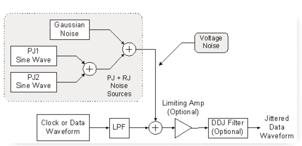
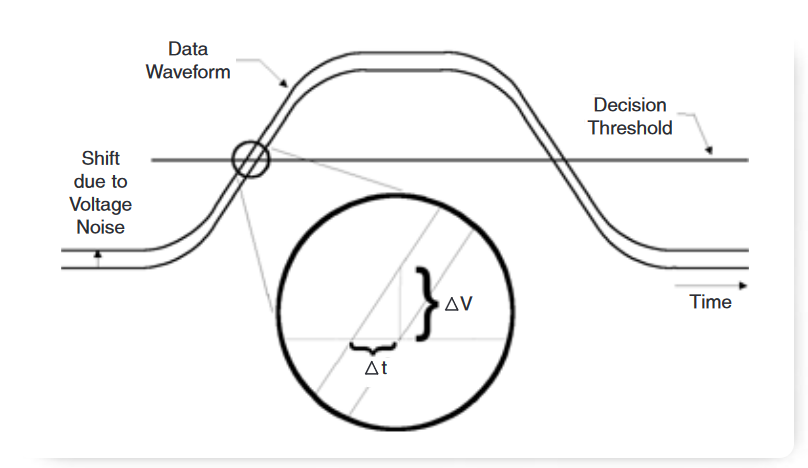
One very broadband way to convert voltage noise into timing jitter is to simply add a noise voltage, using a power combiner, to a data waveform that has modest slew rate on its data edges. This approach is shown in Figure 3, where a low-pass filter has been used to ensure that the edges in the clock or data waveform aren't too fast.
As the noise waveform raises or lowers the data waveform in the region of the edge-detection threshold, it biases the threshold-crossing instant forwards or backwards in time. For example, if the data waveform has edges that rise at 10 V/ns, a 50 mV shift upward in the waveform will cause the threshold to be crossed 5 ps early. Thus, the slew rate of the signal effectively sets the gain of the voltageto-timing conversion. This is depicted in Figure 4. Following the voltage-to-timing conversion, a limiting amp can optionally be used to restore fast edges.
This approach can be useful for adding small amounts of jitter, but you can see that the voltage to timing jitter conversion is only linear if the waveform transition is linear. As the waveform approaches its maximum or minimum, the change in slew rate makes the conversion highly nonlinear. Since random noise has such a high "peak-to-average" ratio, this method should be limited to cases requiring very small amounts of random jitter.
Section 2: Jitter Test Scenarios
2.1 Jitter Tolerance
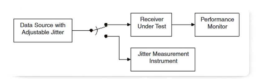
Jitter Tolerance refers to measuring how much timing jitter a device can be subjected to while still maintaining a nominal performance level. The test generally requires a data source with controllable jitter, a means to verify the characteristics of the jittered input signal, and a means to detect whether the receiver-under-test is meeting its performance requirement. A typical block diagram is shown in Figure 5.
Depending on the standard, the jitter on the input signal can take various forms. For example, SONET testing requires jitter in the form of a sinusoidal phase modulation, or PJ, which is swept or stepped across a prescribed frequency band while the amplitude is adjusted according to a compliance mask. This signal is not required to have any particular level of random jitter; in fact, it is assumed to have negligible RJ. The methods reviewed in Section 1.3 can easily meet the need for this kind of testing.
In contrast to SONET testing, the SATA specification requires a test signal bearing a wide variety of both random and deterministic jitter. This kind of test signal cannot be properly produced without attention to detail. In particular, use of an RJ source that has a truncated histogram can lead you to pass a device that will fail in situations where the random jitter noise is more nearly Gaussian. Because of the need for Gaussian distributions that are faithful beyond the 10-12 BER level, many AWGs will not perform sufficiently well.
2.2 Jitter Transfer
Jitter Transfer is a measurement of the amount of jitter present at an output of a device or system, relative to the amount of jitter at a particular input. The ratio is usually specified in the frequency domain, and may be compared to a compliance mask expressed as a Bode plot.
2.2.1 Review of Linear Systems Theory
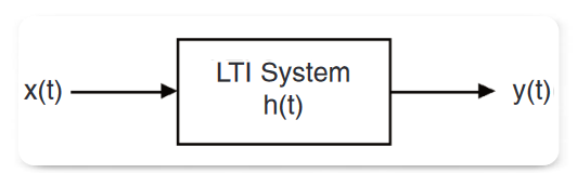
Consider the block diagram of a linear time-invariant system with input x(t), output y(t) and impulse response h(t), as shown in Figure 6.
According to classical linear systems theory, the transfer function of such a system is:
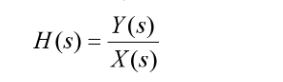
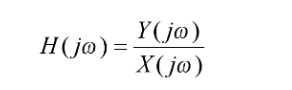
where X(s) is the LaPlace transform of x(t) and s = σ + jω is the complex frequency. For the purposes of measuring the responses of real systems, σ = 0
and the LaPlace transform can be replaced with the Fourier transform. So practically speaking, the transfer function is:
For many purposes the magnitude response adequately describes the situation, leading to the final form for our purposes:
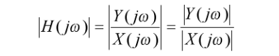
In Figure 6, the signals x(t) and y(t) would conventionally refer to the actual voltage waveforms at these points. However, they can as easily be assigned to mean the time domain jitter modulation at the input and output of the device, respectively. In this case, X(jω) represents the jitter modulation at the input to a device, expressed in the frequency domain, and Y(jω) represents the jitter modulation at the output. According to this interpretation, H(jω) becomes the jitter transfer function.
2.2.2 Setting up a Transfer Function Plot in TDSJIT3 v2.0
Using TDSJIT3 v2.0, it is possible to directly measure the magnitude of the jitter transfer function through a device in many cases. To do so, simultaneously probe the input and output of your device and set up similar measurements (i.e. Data Period measurements) at both points. After performing an acquisition, select Plot>Create to display the various plot choices. In the table at the left side of the user interface, select the measurement corresponding to the output jitter (y(t) in Figure 6) and then choose the Transfer Function button. A dialog box will appear, showing the selected measurement as the numerator of the transfer function equation. For the denominator, choose the measurement corresponding to the input jitter (x(t) in Figure 6), and then select OK.
The resulting plot window shows the frequencydomain magnitude of the output jitter, divided by the magnitude of the input jitter, on log-log axes. Since any real measurement of spectral magnitude is corrupted by a certain amount of noise, the plot will probably show spurious peaks and valleys. To produce a better plot, place TDSJIT3 v2.0 in free-run mode and let it acquire multiple measurements. By default, this plot is configured to average the results of subsequent measurements, and by averaging multiple acquisitions the measurement noise can be greatly reduced. This technique is not limited to devices for which the input and output are at the same rate. This case is discussed in the second example.
2.2.3 Example 1: CDR Characterization
The transfer function can be very useful for characterizing phase locked loops, such as are used in ClockData Recovery (CDR) devices. A properly functioning CDR follows, or tracks, the low-frequency timing variations in its input signal. Timing variations (i.e. jitter) that are well above the loop bandwidth of the CDR are not tracked; at these higher frequencies, the jitter on the output of the device should be controlled by the jitter of the CDR's VCO. In between these two ranges, the PLL (Phase-Locked Loop) may cause jitter peaking.
To plot the jitter transfer curve for a CDR, it is helpful if the input waveform being tracked by the CDR has significantly more jitter noise than the inherent noise of the CDR itself. This jitter should be well distributed over the spectrum (i.e. "white") but it doesn't need to be highly Gaussian. So, this is a case where a general purpose AWG or noise generator can be safely used as the data source.
Since the CDR tracks jitter that is within its loop bandwidth, the transfer function should have a gain of 0 dB at low frequencies. If the CDR's inherent jitter is lower than that of the input signal, the jitter transfer function should break downward at a rate of 20 dB/decade at approximately the PLL bandwidth point. (For a Type2 PLL, the breakpoint will actually be somewhat below the PLL bandwidth. To understand why this is so, see "Characterize Phase-Locked Loop Systems Using Real-Time Oscilloscopes".)
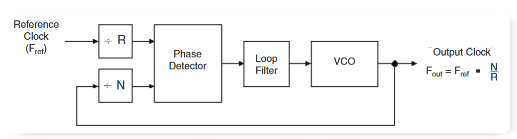
2.2.4 Example 2: PLL Clock Multiplier
Phase-locked loops are frequently used to multiply a reference clock up to a higher frequency, as shown in Figure 7. In theory, the jitter at the output is equal to the jitter on the reference clock multiplied by the divide ratio (in this case, N/R), within the loop bandwidth. Well outside the loop bandwidth, the jitter should be determined by the jitter of the loop's VCO. However, the theory can break down if some other source of jitter, such as power supply noise, creeps into the design.
When jitter is viewed in the frequency domain, the highest jitter frequency that can be viewed is one-half the clock rate. (This is because the phase of the active clock edge can only be sampled once per clock cycle, and the Nyquist theorem says that jitter frequency component higher than this will be aliased down to lower frequencies.)
Using TDSJIT3 v2.0, you can plot the transfer function of jitter on Fout versus jitter on Fr. To do this, set up one TIE measurement on the input and another on the output, and then plot TIEout/TIEref When the clock rates of the numerator and denominator are different, TDSJIT3 v2.0 automatically uses the lower of the two rates to determine the right-hand limit for the frequency axis.
As in the last example, you may wish to use an intentionally modulated clock to explore how your PLL transfers jitter from input to output. And as before, this kind of test does not place extreme demands on the jitter generation.
2.3 Test Equipment Verification
There are numerous jitter measurement systems available today, varying widely in price, convenience, flexibility, technical competence and claimed performance. One of the most challenging tasks for any design or qualification engineer is to compare the available solutions and choose the best one for their application. An important aspect of this choice is assessing the instruments or systems for accuracy and repeatability
One approach to verifying performance claims is to compare an instrument's jitter results to those of a trusted reference instrument, typically a BERT. Although this is generally a sound approach, even BERTs have sources of error. As the art and science of jitter measurement has matured, the use of a BERT as a final arbiter has increasingly been questioned.
Another approach to verifying performance is to create a signal for which the true jitter is "known," and compare the measured results to the expected values. Since there is no accepted reference standard for jitter, there is little technical guidance available in this area for the would-be evaluator. Unfortunately, there are far more ways to do things wrong than to get everything right. This task is really the torture test of jitter generation, and you cannot take anything for granted. All of the comments in Section 1 regarding verification of probability distributions and frequency and phase deviations should be taken seriously if you venture into this realm.
TDSJIT3 v2.0 uses the basic assumption that jitter is a statistical result of many single shot time measurements. Thus, using the base instrument accuracy specification for indivdual measurements allows the composite jitter accuracy to be inferred. The difficulty comes when specifying accuracy of the decomposition method, or accuracy of separated RJ and DJ results. Using the spectral decomposition method allows for a direct view of the various jitter components and is considered the most accurate method available, with sensitivity to the base instrument noise floor the major fallibility true of all methods.
Summary
When characterizing jitter performance, it may be useful or mandatory to have a signal source with intentional jitter of known characteristics. This deceptively simple goal can be surprisingly difficult to achieve. Fortunately, many practical cases don't demand metrology-grade jitter. By understanding which jitter characteristics are important in each application, you can use the equipment that economically meets the need when possible, and avoid expensive mistakes in those cases where the easy approach isn't adequate
Using the spectral decomposition method allows for a direct view of the various jitter components and is considered the most accurate method available. As with all implementations, the noise floor of the measurement hardware bounds the practical limit of attainable performance.
Appendix A: Verifying a Gaussian Voltage Waveform
The following procedure can be used to check a nominally Gaussian noise source, to verify how faithfully its amplitude distribution matches the theoretical Gaussian curve. The procedure consists of the two steps of data acquisition and analysis. It requires a high-performance oscilloscope and access to the MATLAB* analysis application.
The data acquisition is described as it would be performed on a Tektronix TDS5000-, 6000-, or 7000- series oscilloscope, but the same technique may be useable, with suitable modifications, on other oscilloscopes capable of measuring and exporting histograms.
The analysis is by means of a MATLAB script. The instructions that follow are intended to allow even a person who is not familiar with MATLAB to successfully perform the analysis.
A.1: Data Acquisition
Since the goal is to verify the amplitude distribution of the noise source, the noise source output should be attached directly to channel 1 of the oscilloscope. The oscilloscope sample rate should be set several times higher than the nominal bandwidth of the noise source, and the vertical sensitivity should be set so that the waveform peaks on a typical acquisition span no more than 25% - 35% of the oscilloscope's digitizer range. This is to allow the occasional higher peaks to be captured without clipping. The waveform length may be set as desired, but longer record lengths will accumulate statistics more rapidly than will short records.
The following steps can be used to set up the histogram measurement:
1. Adjust the oscilloscope vertical and horizontal sensitivities and record length as described above. Turn on vertical bar cursors and use them to find the time positions that correspond to the extreme left end and right edges of the graticule. Similarly, use horizontal-bar cursors to find the voltages corresponding to the top and bottom of the graticule.
2. Set the oscilloscope top bar to "Menu" mode (rather than "Buttons"), and select Measure>Waveform Histograms… Set the waveform source to Ch1 and the histogram mode to "Vert". The histogram scaling should be set to log since this will allow the Gaussian tails to be seen more clearly; note that the exported data will be linear in any event. Set the Left Limit and Right Limit controls to the time values for the left and right edges of the graticule, as found in step one. Similarly, set the Top Limit and Bottom Limit to match the voltages at the top and bottom of the graticule. The histogram box now includes the entire visible screen, and the histogram should be visible at the left side of the graticule.
3. Let the oscilloscope run for some time in free-run mode. Typically an overnight or longer run is required to accumulate statistics that approach the 7-sigma level. If the noise source deviates significantly from Gaussian, a much shorter run will probably reveal it.
4. Export the acquired histogram. Select File>Export Setup… and go to the Measurements tab. Select the Histogram Data (CSV) radio button, and choose Export. This will save an ascii text file with two columns. The first column contains the bin values (in this case in volts) for the histogram. The second column contains the populations for the corresponding bins.
A.2: Data Analysis
The data is analyzed in MATLAB, using the script "check_gaussian_match.m", found at the end of this appendix. Use the following procedure:
1. Place the exported histogram file and the MATLAB script in a convenient working directory. Start the MATLAB application, and navigate to the working directory by using the browse button ("…") in the upper right corner beside the current directory path.
2. At the MATLAB prompt, type:
>> load filename.csv –ascii
where >> is the MATLAB prompt and filename.csv is the actual name that you used. This should load the histogram data into the MATLAB workspace, using the filename as the name of the data matrix. You can confirm the name of the matrix by typing:
>> whos
which will cause a summary of all loaded data objects to be displayed.
3. Rename the histogram data to "my_hist", since that is what the analysis script expects. To do this, type:
>> my_hist = filename;
This will create a copy of the histogram with the name "my_hist".
4. At the MATLAB prompt, type:
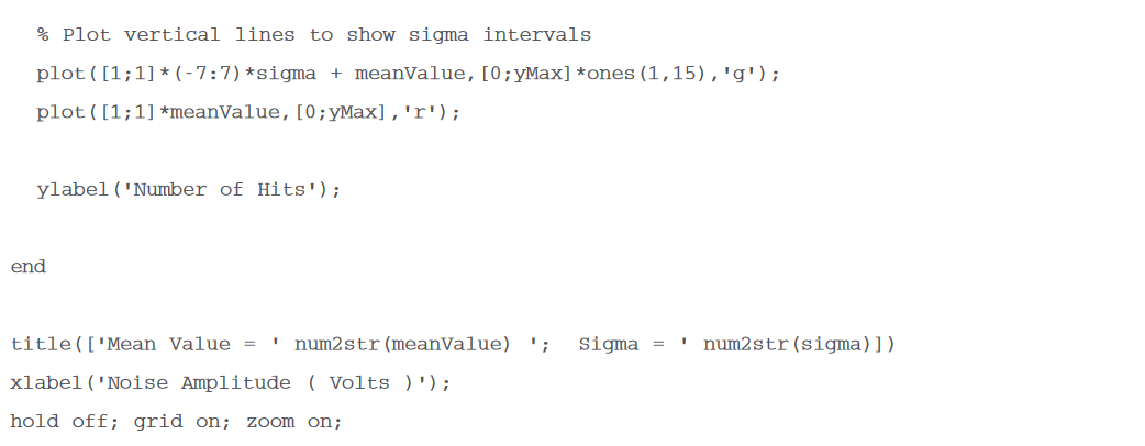
>> check_gaussian_match
This will cause the analysis script to run. The result should be a plot that shows the actual measured histogram in blue and the best-fit Gaussian curve in red. Vertical lines show the mean and the ±1, ±2, … ±7 sigma points. Significant deviation between the two curves (i.e. due to compression in the output amplifier of the noise source) should be obvious, and the range over which the noise source is Gaussian can be seen.
If you are familiar with MATLAB or just adventurous, you can explore the analysis script with any text editor and consider modifying it.
A.3: Technical Notes
The theoretical Gaussian curve is found by performing a curve fit of the function:
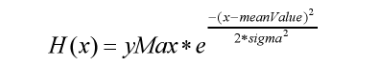
against the measured histogram data, after each histogram point has been weighted according to its population.
The three parameters yMax, sigma, and meanValue are all adjusted to find the best curve fit. (The leading term of yMax replaces the usual term of 1/(sigma*sqrt(2*pi)) to account for the normalization factor between a histogram and a pdf.) The curve-fitter is an unconstrained nonlinear minimizer of the meansquared error between the weighted histogram points and the theoretical Gaussian curve.
A.4: MATLAB Script