
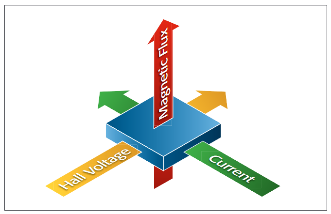
The Hall effect can be observed when the combination of a magnetic field through a sample and a current along the length of the sample create an electrical current perpendicular to both the magnetic field and the current, which in turn creates a transverse voltage perpendicular to both the field and the current (Figure 1). The underlying principle is the Lorentz force: the force on a point charge due to electromagnetic fields
Hall effect measurements are invaluable for characterizing semiconductor materials whether they are silicon-based, compound semiconductors, thin film materials for solar cells, or nanoscale materials like graphene. The measurements span low resistance (highly doped semiconductor materials, high temperature superconductors, dilute magnetic semiconductors, and GMR/TMR materials) and high resistance semiconductor materials, including semi-insulating GaAs, gallium nitride, and cadmium telluride.
A Hall effect measurement system is useful for determining various material parameters, but the primary one is the Hall voltage (VH). Carrier mobility, carrier concentration (n), Hall coefficient (RH), resistivity, magnetoresistance (RB), and the carrier conductivity type (N or P) are all derived from Hall voltage.
As researchers develop next-generation ICs and more efficient semiconductor materials, they‘re particularly interested in materials with high carrier mobility, which is what's sparked much of the interest in graphene. This one-atom-thick form of carbon exhibits the quantum Hall effect and, as a result, relativistic electron current flow. Researchers consider Hall effect measurements crucial to the future of the electronics industry
Materials with high carrier mobility allow creating devices that obtain maximized current flow at lower power levels with faster switching times and higher bandwidth. A manipulation of Ohm's Law (Figure 2) shows the importance of carrier mobility in maximizing current. The current is directly proportional to carrier mobility
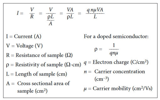
The options for maximizing current flow through a device include increasing voltage, charge carrier concentration, the cross-sectional area of the sample, or the mobility of the charge carriers. All but the last of these have serious disadvantages.
Measuring Mobility
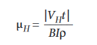
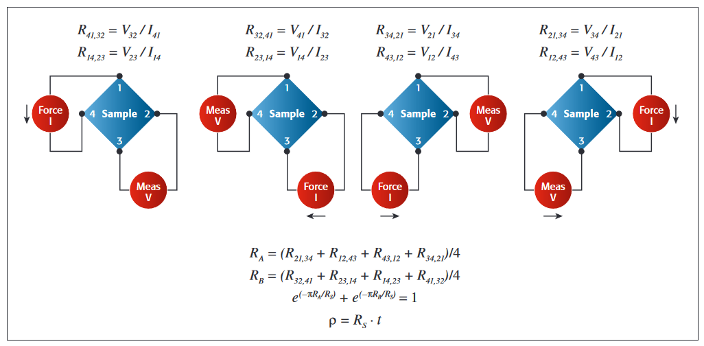
The first step in determining carrier mobility is to measure the Hall voltage (VH) by forcing both a magnetic field perpendicular to the sample (B) and a current through the sample (I). This combination creates a transverse current. The resulting potential (VH) is measured across the device. Accurate measurements of both the sample thickness (t) and its resistivity (r) are also required. The resistivity can be determined using either a four-point probe or the van der Pauw measurement technique. With just these five parameters (B, I, VH, t,and resistivity), the Hall mobility can be calculated:
Both Hall voltages and the measured van der Pauw resistivity are typically quite small, so the right measurement and averaging techniques are critical for accurate mobility results.
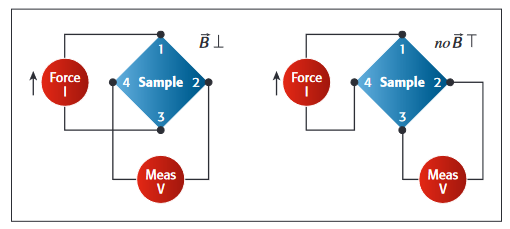
Figure 3 illustrates the measurement configurations for both the Hall voltage and the van der Pauw resistivity measurement. The two measurement configurations both use four contacts and involve forcing a current and measuring a voltage. However, in addition to different connection schemes, the Hall voltage measurements require a magnetic field.
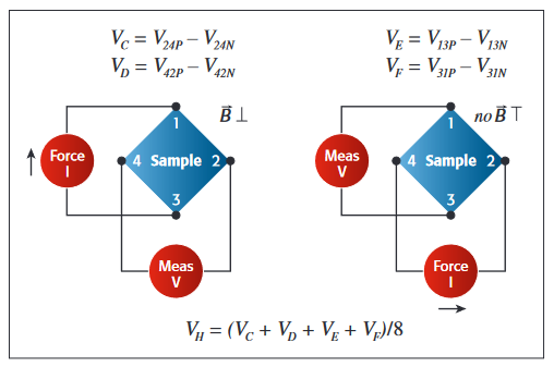
Hall voltages and van der Pauw voltages can be as low as millivolts, so the recommended test technique involves a combination of reversing source current polarity, sourcing on additional terminals, and reversing the direction of the magnetic field. Eight Hall effect and eight van der Pauw measurements are performed. If the voltage readings within each measurement differ substantially, always recheck the test setup for sources of error
A basic Hall effect measurement configuration will likely include the following components and optional extras:
- A bipolar, constant-current source. For low resistivity samples, it must be able to source from milliamps to amps. For high resistivity samples (107 ohm·cm or higher), a sourcing range as low as 1nA will be needed.
- A high input impedance voltmeter. Depending on the resistivity under test, the voltmeter used must be able to measure voltages from 1 microvolt to 100V accurately. High resistivity materials may require ultra-high input impedance or differential measurements
- A permanent magnet or an electromagnet capable of generating field magnitudes from 500 to 5000 gauss.
- A sample holder
- Optional equipment. A switch matrix helps to eliminate the need for manual connections/disconnections between probe contacts. A switch matrix is definitely required if the sample is in a liquid nitrogen dewar for temperature studies. Hall measurements are highly dependent on sample temperature, so it is often important to monitor this temperature. A prober chuck that can either heat or cool the sample and a temperature controller are generally necessary for on-wafer measurements when doing temperature studies.
The most appropriate Hall effect measurement instruments will be based on the total resistance of the sample and the resistance of its external contact points. The sample resistance is the sample's intrinsic resistivity, expressed in units of ohm-centimeters (ohm·cm) divided by its thickness. The contact resistance to the sample can be orders of magnitude higher than the sample's resistance. The measurement system might be designed to accommodate samples with a wide range of resistances or optimized specifically for studying low resistance (narrow bandgap) or high resistance (wide bandgap) materials.
A Wide Resistance Measurement System
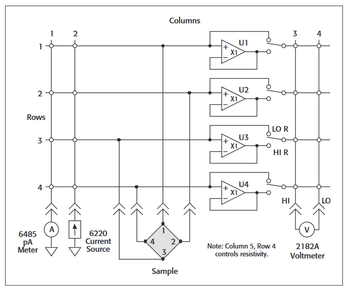
Figure 6 shows a Hall effect/van der Pauw measurement system appropriate for sample resistances ranging from 1µΩ to 1TΩ. It employs Keithley's Model 7065 matrix switching card optimized for Hall effect measurements housed in a Model 7001 Switch Mainframe. This card buffers test signals from the sample to the measurement instrumentation and switches current from the current source to the sample. It offers the advantage of unity gain buffers that can be switched in and out to allow measuring high resistances by buffering the sample resistance from the meter.
The test setup also includes a Model 6485 picoammeter, Model 6220 DC current source, and Model 2182A nanovoltmeter. The picoammeter is included as an option for monitoring system leakage currents. The current source and nanovoltmeter work together using internal techniques to synchronize their operation, eliminate thermal offsets, and improve measurement accuracy. The nanovoltmeter's second voltage measurement channel is useful for monitoring the sample temperature.
Enhancing Hall Effect Measurement Confidence
Building good measurement practices into a Hall effect system's design will enhance its measurement integrity:
- Always incorporate electrostatic shielding to minimize electrical interference. Electrostatic coupling or interference occurs when an external electric field injects error signals into the circuit under test. Minimize this by shielding the sample and all sensitive measurement circuitry, connecting the shield to the test system's low reference, and using shielded cabling. For more on shielding, consult Section 2 of Keithley's Low Level Measurements Handbook.
- Ensure the test system is properly grounded. Prevent ground loops by grounding all equipment in the test system at a single point, the circuit reference common point.
- Use guarding to reduce the effects of leakage current. This includes the use of a guarded current source, guarded voltmeter, and triaxial rather than coaxial cables.
- Allow sufficient settling time before making measurements. When measuring a high resistance sample, the capacitance in the cabling combined with the high resistance sample creates a large RC time constant, requiring significant time for the voltage to stabilize. To determine the amount of delay time needed, monitor the voltage as a function of time.
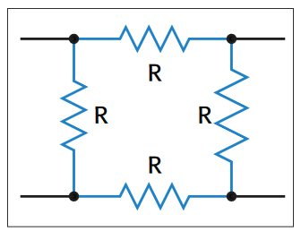
- Regularly verify the system's performance. The simplest way to do this is to build a test structure using four resistors of equal value of similar magnitude to the sample's resistance (Figure 7). Compare measurements on the test structure with expected results
- Minimize sources of thermoelectric voltages. Whenever possible, use the same materials in all connections, such as all-copper connections and copper wire. Reverse the current source's polarity and average the readings to eliminate EMF errors. Always allow the test equipment to reach thermal equilibrium before starting testing, and minimize temperature gradients across the sample.
Conclusion
Characterizing the mobility of new materials is essential to semiconductor technology innovations, so making accurate Hall effect measurements will continue to be important. For more information and additional system configurations, view the Keithley online webinar, "Hall Effect Measurement Fundamentals," available on Keithley's website at http://www.keithley.com/events/semconfs/webseminars.