
Introduction
Carbon nanotubes (CNTs) have been the subject of a lot of scientific research in recent years, due not only to their small size but to their remarkable electronic and mechanical properties and many potential applications. The problems associated with attempting to scale down traditional semiconductor devices have led researchers to look into CNT-based devices, such as carbon nanotube field effect transistors (CNT FETs), as alternatives. Because they are not subject to the same scaling problems as traditional semiconductor devices, CNT FETs are being studied for a wide variety of applications, including logic devices, memory devices, sensors, etc. The research on these devices typically involves determining various electrical parameters, which may include current-voltage (I-V), pulsed I-V, and capacitance (C) measurements. Characterizing the electrical properties of delicate nanoelectronic devices requires instruments and measurement techniques optimized for low power levels and high measurement sensitivity.
The Model 4200-SCS Semiconductor Characterization System offers a variety of advantages for electrical characterization of CNT FETs. This configurable test system can simplify these sensitive electrical measurements because it combines multiple measurement instruments into one integrated system that includes hardware, interactive software, graphics, and analysis capabilities. The system comes with pre-configured tests for performing electrical measurements that have been optimized to ensure accurate results on CNT FETs. This application note explains how to optimize DC, pulsed I-V, and C-V measurements on a CNT FET using the Model 4200-SCS Semiconductor Characterization System. It includes detailed information on proper cabling and connections, guarding, shielding, noise reduction techniques, and other important measurement considerations when testing carbon nanotube transistors.
The Carbon Nanotube Transistor
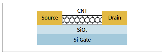
A single semiconducting CNT can be used as the conducting channel between the source and drain of a FET.Figure 1 illustrates a back-gated Schottky barrier CNT FET. Two metal contacts are located across both ends of the CNT to form the Source and Drain terminals of the FET. The CNT is placed atop an oxide that sits above a doped silicon substrate, which forms the Gate terminal. Connections are made to the three DUT terminals to perform the electrical measurements.
Making Electrical Measurements with the Model 4200-SCS
The Model 4200-SCS is supplied with a test project for making some of the most commonly used CNT FET measurements. This project (CNTFET) includes tests for I-V, pulsed I-V, and C-V measurements. The I-V tests are performed using two of the Model 4200-SMU Source Measure Units, both with the Model 4200-PA Preamp option. The pulsed and transient I-V measurements are made using the Model 4225-PMU Ultra Fast I-V Module with two Model 4225-RPM Remote/Preamplifier Switch options. Finally, the C-V measurements are performed using the Model 4210-CVU C-V Measurement module.
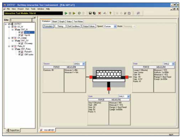
The CNTFET project is included with all Model 4200-SCS systems running KTEI Version 8.1 or later. Figure 2 shows the CNTFET project running in the Keithley Interactive Test Environment (KITE) software.
Current-Voltage Measurements
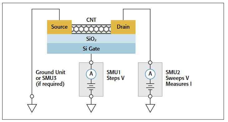
The I-V characteristics of a CNT transistor can be used to extract many of the device's parameters, study the effects of fabrication technique and process variations, determine the quality of the contacts, etc. Figure 3 illustrates a DC I-V test configuration that incorporates two Model 4200-SMUs (Source Measure Units). These SMUs are capable of sourcing and measuring both current and voltage; they have picoamp sensitivity and can be current-limited to prevent damage to the device. In this diagram, SMU1 is connected to the Gate of the CNT FET and SMU2 is connected to the Drain. The Source terminal is connected to the Ground Unit (GNDU) or to a third SMU if it is necessary to source and measure from all three terminals of the FET.
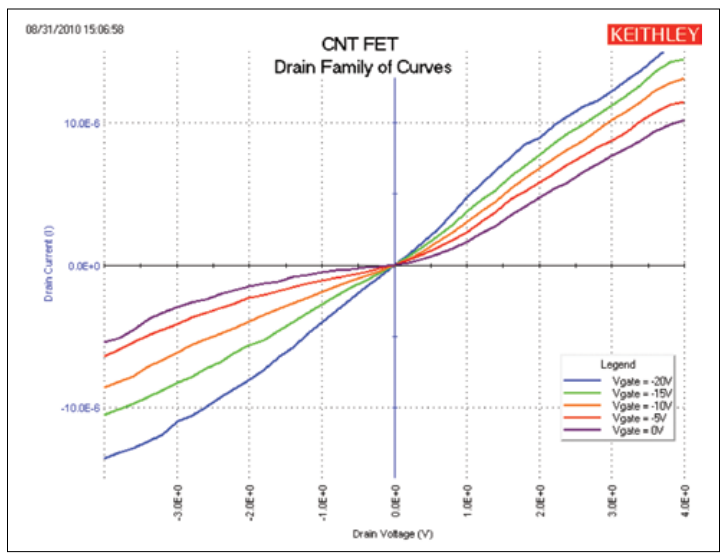
In this example, the Model 4200-SCS's KITE software is set up to measure a DC drain family of curves (Vds–Id). As SMU1 steps the gate voltage (Vg), SMU2 sweeps the drain voltage (Vd) and measures the resulting drain current (Id). Figure 4 shows the resulting FET characteristics generated using the CNTFET project.
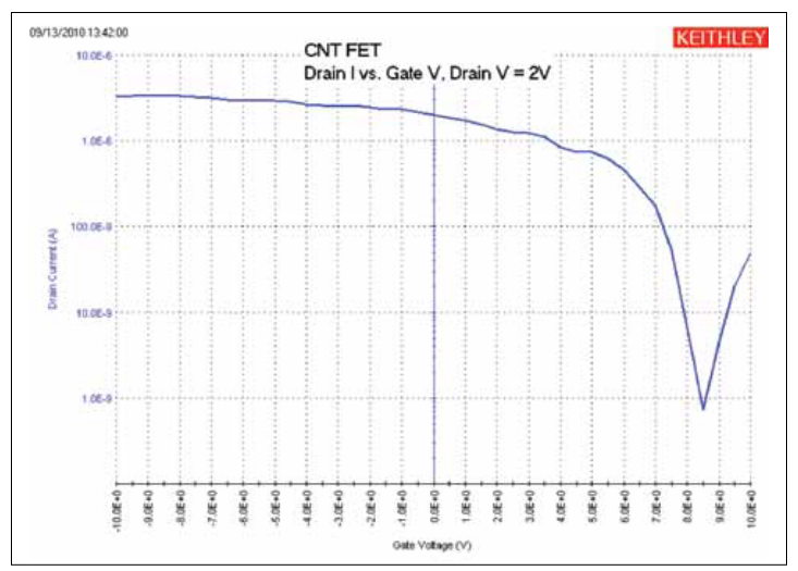
Without changing connections to the device, 4200-SCS's interactive KITE software simplifies performing other common I-V tests such as the drain current (Id) vs. gate voltage (Vg) curves. For this test, the gate voltage is swept and the resulting drain current is measured at a constant drain voltage. The results of an Id–Vg curve at a constant drain voltage are shown in Figure 5. The drain voltage can also be stepped as the gate voltage is swept.
Optimizing DC measurements
The following techniques will improve the quality of DC measurements made on CNT FETs with the Model 4200-SCS:
- Limit Current: To prevent damage to the device while performing I-V characterization, the user should limit the amount of current that can flow through the device. This can be done in the software by setting the Current Compliance of each SMU to a safe level, such as 20µA. This is a programmed limit to ensure the current doesn't exceed the user-defined compliance.
- Provide Sufficient Settling Time: Because CNT FET measurements often involve measuring low current (<1µA), it is important to allow sufficient settling time to ensure the measurements are stabilized after a current or voltage has been applied. Some of the factors that affect the settling time of the measurement circuit include the cables, test fixtures, switches, probers, the DUT resistance, and the current range of the measurement instrument. To ensure settled readings, additional delay time can be added to the voltage or current step time prior to the measurement. This delay time can be easily adjusted in the Timing Menu in the KITE software.
- Use Proper Speed Modes: The Timing Menu also offers Speed Modes, including Delay and Filter Factor settings, which affect the settling time of the reading, as well as the integration time of the measurement. Increasing the Delay Factor, Filter Factor, and the A/D Aperture Time can decrease noisy measurements.
- Minimize Noisy Measurements: Noise may be generated from a variety of sources, including particle collisions, defects, AC pick-up, and electrostatic interference. Noisy measurements result when a noise signal is superimposed on the DC signal being measured. This can result in inaccurate or fluctuating measurements.
The most common form of external noise "pick-up" is 60Hz (or 50Hz) line cycle pick-up. This can be a common occurrence near fluorescent lights. Millivolts of noise are not uncommon. Keithley uses a technique called LineCycle Integration to minimize the effects of 60Hz (or 50Hz) line pick-up. Line-cycle noise will "average out" when the integration time is equal to an integral number of power line cycles. The number of power line cycles can be adjusted in the KITE software in the Timing Menu.
Electrostatic interference is another cause of noisy measurements when measuring low currents. This coupling occurs when an electrically charged object approaches the circuit under test. In high impedance circuits, this charge doesn't decay rapidly and can result in unstable measurements. The erroneous readings may be due to either DC or AC electrostatic fields, so electrostatic shielding will help minimize the effects of these fields.
The electrostatic shield can be just a simple metal box that encloses the test circuit. Probe stations often include an electrostatic/EMI shield or optional dark box. The shield should be connected to the measurement circuit LO, which is the Force LO terminal of the SMU. The Force LO terminal is the outside shield of the triax cable of the SMU or is located on the GNDU. All cables need to be of a lownoise design and shielded. Each Model 4200-SMU comes with two low-noise triax cables.
- Keep Probes Up: Make sure the probes are in the up position (not contacted to the device) when connecting and disconnecting instruments from the terminals of the device. The process of moving cables has the potential to inject charge into the device and cause damage. This is due to both triboelectric and piezoelectric effects.
Pulsed I-V Measurements
In addition to making traditional DC I-V measurements, it may be desirable to perform ultra-fast pulsed I-V measurements for various reasons. First, it may be important to observe the high speed response of the CNT device. In some cases, nanostructures can be destroyed by the heat generated when making traditional DC measurements. Pulsed I-V measurements can reduce the total energy dissipated in a device, and therefore reduce the potential for damage. Finally, pulsed electrical testing can prevent current drifting in measurements that can occur during DC measurements.
The pulsed I-V measurements on the CNT FET can be easily made using the Model 4225-PMU Ultra Fast I-V Module. The Model 4225-PMU provides two channels of high speed, multilevel voltage pulse output while simultaneously measuring current and voltage. This module replaces traditional pulse/ measure test configurations, which consisted of a pulse generator, digital oscilloscope, interconnect hardware, and software.
The Model 4225-PMU has two modes of ultra-fast I-V source with measure: pulsed I-V and transient I-V. These two modes are illustrated in Figure 6.
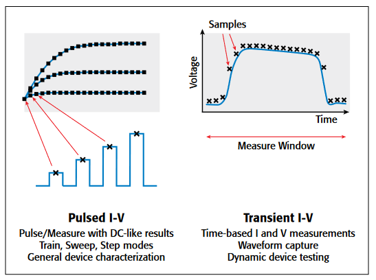
Pulsed I-V refers to any test with a pulsed source and a corresponding high speed, time-based measurement that provides DC-like results. The current and/or voltage measurement is an average of readings taken in a predefined measurement window on the pulse. This average of readings is called the "spot mean." The user defines the parameters of the pulse, including the pulse width, duty cycle, rise/fall times, amplitude, etc.
Transient I-V, or waveform capture, is a time-based current and/or voltage measurement that is typically the capture of a pulsed waveform. A transient test is typically a single pulse waveform that is used to study time-varying parameters, such as the drain current degradation versus time due to charge trapping or self-heating. Transient I-V measurements can be used to test a dynamic test circuit or as a diagnostic tool for choosing the appropriate pulse settings in the pulsed I-V mode.
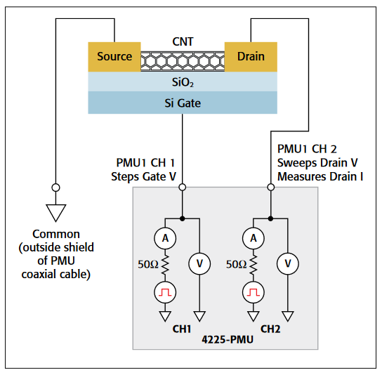
Given that the 4225-PMU has two channels, only one module is needed to test a three-terminal CNT FET. A typical test configuration for connecting the PMU module to a CNT FET is shown in Figure 7. In this diagram, Ch 1 of the PMU is connected to the Gate terminal and Ch 2 is connected to the Drain terminal. The Source terminal is connected to the PMU Common, which is the outside shield of the PMU coax connector. To connect this Common terminal to the probe tip, use a BNC or triax shorting plug that will connect the outside of the coax to the manipulator probe. To generate a Vds–Id curve, Ch 1 steps the gate voltage and Ch 2 sweeps the drain voltage and measures the resulting drain current.
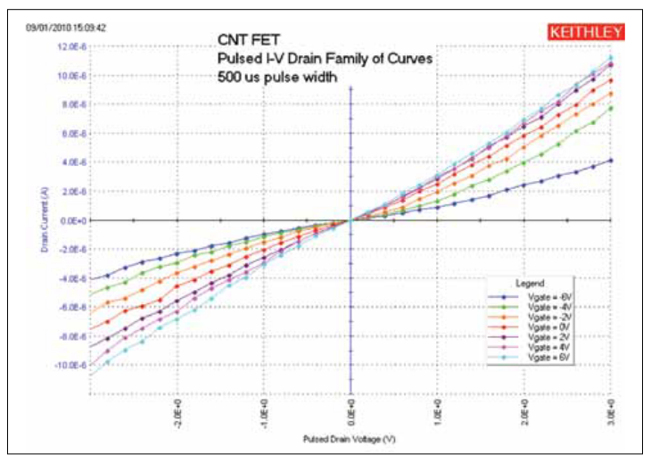
Figure 8 illustrates a pulsed I-V drain family of curves taken with the Model 4225-PMU. For this measurement, a pulse width of 500µs was used to generate the curves. However, each PMU channel has the ability to output voltage pulses as short as 70ns with a rise time as short as 20ns. The minimum duration of the pulse width will depend on several factors, including the test circuit RC time constant and the magnitude of the test current. Each dot on the curves represents a "spot mean" measurement on the pulsed waveform.
The Model 4225-PMU has five ranges full scale from 800mA down to 100µA. To measure lower currents, using the Model 4225-RPM optional Remote Amplifier/Switch is recommended because it adds six measurement ranges, down to 100nA full scale. The pulsed I-V curves shown in Figure 8 were taken on the 100µA range. The threshold current was set to 20µA so that the test will stop if the threshold current level is reached.
For some applications, it may be necessary to study the transient response of a CNT FET. If this is the case, the waveform capture mode (transient I-V) can be used to capture the current and voltage time-based response to the device. Figure 9 shows the transient response of the CNT FET. The blue curve is the pulsed drain voltage and the red curve is the resulting current response as a function of time.
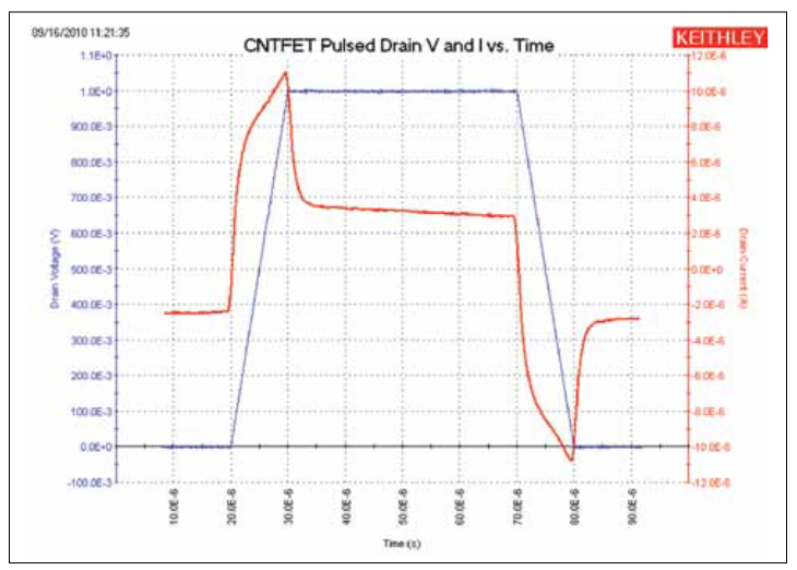
The blue voltage output curve looks close to the defined rise and fall times of 10µs with a pulse width of 50µs. Note that the pulse width is measured at one-half of the input amplitude of 1V. Therefore, the pulse width is measured at 500mV. The sample period in this example is 25ns (40MHz rate). With proper cabling and connections, the voltage shape should be output as defined by the user with minimal deviation.
The red curve shows the drain current and is plotted on the right Y-axis. The drain current is measured at constant drain and gate voltages. The peaks in the curve are caused by charging and discharging of the cabling, as well as the current flow through the device. Note that these peaks occur during the pulse transitions. Reducing the pulse amplitude or increasing the pulse transition time reduces the dV/dt, which reduces the peak height.
Optimizing Pulsed I-V Measurements
To improve the quality of pulsed I-V measurements made with the Model 4200-SCS, follow these guidelines:
- Use the Right Cables and Connections: Using proper cabling and connections is important for ultrafast I-V applications in order to achieve the highest frequency output and to avoid signal distortions and capacitive charging effects.
- Use cabling and connections optimized for high frequency (at least 150MHz).
- Use a signal path that matches the impedance of the instrument (50 ohms).
- Tie the low side of the DUT to the shield of the PMU coax cable.
- Connect the shields from each PMU channel together as close as possible to the DUT.
- Minimize the loop area once the center conductor and shield are separate in the test circuit.
- Minimize the cable length.
- Make the Right Chuck Connections: CNT FETs and other nanotransistors may be either back-gated or top-gated. For back-gated devices, one of the PMU channels needs to be connected to the chuck of the prober. When making PMU connections to the chuck, the user will give up some functionality of the PMU: fast transitions, high frequency, low current, etc. This is because the output of the high frequency PMU channel is connected to the chuck capacitance and the chuck cabling, which slows down the source response and couples noise into the measurement. If possible, it is better to use a third manipulator and probe directly to the chuck. For high speed sourcing and measuring, it is best to use all top-side connections and avoid connecting the PMU to the chuck.
- Verify Pulse Width: Ensure the pulse width is long enough to ensure a settled reading. Verify the resulting current measurement is settled by outputting a single pulse using the Waveform Capture mode. Both the current and voltage can be plotted as a function of time in the Graph tab.
- Minimize Noise: To minimize noisy results, multiple waveforms can be averaged or a moving average function can be created in the built-in Formulator to smooth out the measurements further.
Capacitance-Voltage Measurements
In addition to performing DC and pulsed I-V measurements on CNT FETs, measuring the capacitance of the FET can also provide information about the device, including the mobility, timing effects, and gate dielectrics. Figure 10 outlines the connections of the Model 4210-CVU to the CNT FET. In this configuration, the gate-to-drain capacitance is measured as a function of the gate voltage.
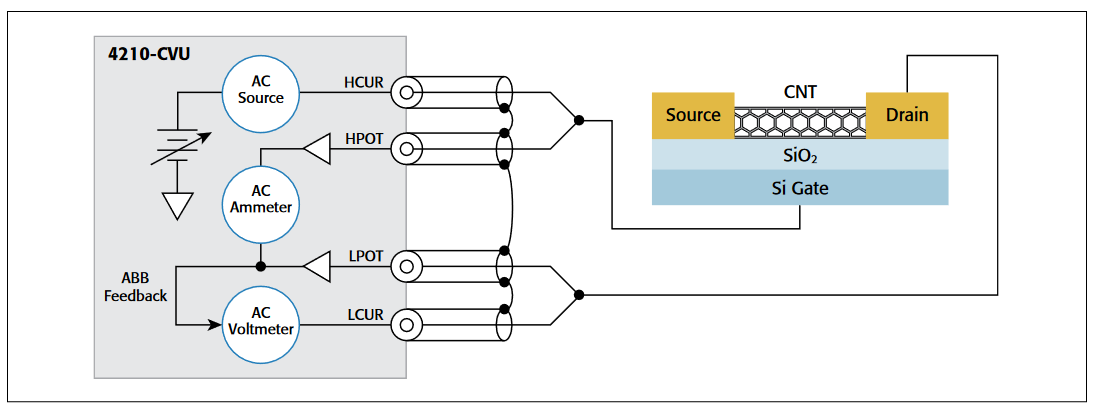
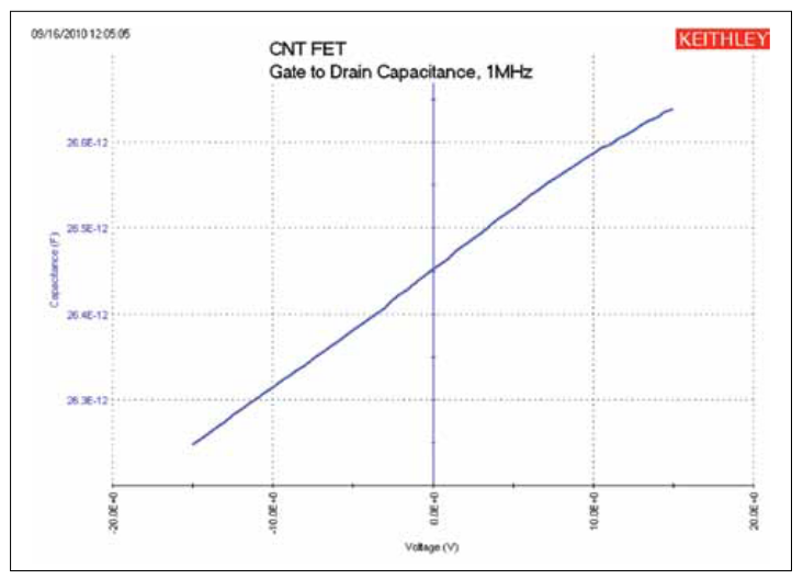
The HCUR/HPOT terminals that connect the high of the voltage source to the gate should be connected to the chuck. The LCUR/LPOT terminals that measure the capacitance should be connected to the drain terminal of the DUT. For best results, the measurement terminals should never be connected to the chuck. For top-gated CNT FETs, both the measure and voltage source can be output to the gate of the FET from the same terminals (either HCUR/HPOT or LPOT/ LCUR) of the CVU. The HI and LO terminals of the CVU are interchangeable in the Force Measure Window of the CVU in the KITE software. The results of generating a C-V sweep between the gate and drain of the CNT FET are shown in Figure 11.
Optimizing Capacitance Measurements
To improve the quality of capacitance measurements made with the Model 4200-SCS, follow these guidelines:
- Perform Open Compensation (for Measurements <10pF): The open correction feature compensates for capacitance offsets in the cabling and connections. Performing the correction is a two-part process. The corrections are performed, and then they are enabled within a test module. To perform the corrections, open the Tools Menu and select CVU Connection Compensation. For an Open correction, click on Measure Open. Probes must be up or the DUT removed from the test fixture. Enable the correction by clicking on the Compensation button in the Forcing Functions/Measure Options window.
- Use Proper Shield Connections: Connect the shields of the coax cables together as close as possible to the DUT. This reduces the loop area of the shields, which minimizes the inductance. This also helps to maintain the transmission line effects. If the shields are not connected together, offsets may occur. The higher the frequency, the more important this becomes.
- Choose Appropriate Hold and Sweep Delay Times: The condition of a device when all internal capacitances are fully charged after an applied voltage step is referred to as "equilibrium." If capacitance measurements are made before the device is in equilibrium, inaccurate results may occur.
To choose the delay times for a C-V sweep, step an applied voltage using the Sampling Mode, and plot the capacitance as a function of time. Observe the settling time from the graph. Use this time for the Hold Time for the initial applied voltage or for the Sweep Delay Time applied at each step in the sweep. The Sweep Delay Time may not need to be as long as the first step. The user will need to experiment to verify the appropriate time. - Choose Appropriate Speed Mode in Timing Menu: The Speed mode function enables the user to adjust the time for settling and integration of the measurement. For small capacitances (pico-Farads or less) use the Quiet or Custom Speed modes for best results.
- Use Guarding: When making very small capacitance measurements, guarding will help prevent stray capacitance from unused terminals of the device from affecting measurement accuracy. For example, if measuring the capacitance between only the gate and drain terminals, the source terminal of the FET can be connected to the guard. The guard terminal of the Model 4210-CVU is the outside shield of the coax cable.
Conclusion
When using the appropriate instrumentation and measurement techniques, optimal electrical characterization of CNT FETs can be achieved. The Model 4200-SCS is an ideal tool for performing electrical characterization of CNT FETs and other nanostructures because of its integrated hardware, software, and analysis tools. The Model 4200-SMU Source Measure Unit can be used to determine Vds–Id, VGS–Id, resistance, and other I-V measurements on the CNT FET. The Model 4225-PMU Ultra-Fast I-V Module can be used to make pulsed I-V measurements or observe the transient response of a pulsed waveform applied to the DUT. The Model 4210-CVU Capacitance Meter can be used to generate C-V, C-f, or C-t curves. Using the CNTFET project that comes with the Model 4200-SCS can further simplify measurement setup and execution.