Contact us
Call us at
Available 6:00 AM – 5:00 PM (PST) Business Days
Download
Download Manuals, Datasheets, Software and more:
Feedback
ABCs of Probes Primer
ABCs of Probes Primer
Learn about the fundamentals of probes and discover how to choose the right probe for your oscilloscope and get reliable measurements every time in this comprehensive ABCs of Probes primer.
= = = = = = = = = = = = = =
1. Probing Safety
Safety Summary
When making measurements on electrical or electronic systems or circuitry, personal safety is of paramount importance. Be sure that you understand the capabilities and limitations of the measuring equipment that you’re using. Also, before making any measurements, become thoroughly familiar with the system or circuitry that you will be measuring. Review all documentation and schematics for the system being measured, paying particular attention to the levels and locations of voltages in the circuit and heeding any and all cautionary notations.
Additionally, be sure to review the following safety precautions to avoid personal injury and to prevent damage to the measuring equipment or the systems to which it is attached. For additional explanation of any of the following precautions, please refer to Explanation of Safety Precautions.
- Observe All Terminal Ratings
- Use Proper Grounding Procedures
- Connect and Disconnect Probes Properly
- Avoid Exposed Circuitry
- Avoid RF Burns While Handling Probes
- Do Not Operate Without Covers
- Do Not Operate in Wet/Damp Conditions
- Do Not Operate in an Explosive Atmosphere
- Do Not Operate with Suspected Failures
- Keep Probe Surfaces Clean and Dry
- Do Not Immerse Probes in Liquids
Explanation of Safety Precautions
Review the following safety precautions to avoid injury and to prevent damage to your test equipment or any product that it is connected to. To avoid potential hazards, use your test equipment only as specified by the manufacturer.
Keep in mind that all voltages and currents are potentially dangerous, either in terms of personal hazard, damage to equipment, or both.
Observe All Terminal Ratings
- To avoid fire or shock hazard, observe all ratings and markings on the product. Consult the product manual for further ratings information before making connections to the product.
- Do not apply a potential to any terminal that exceeds the maximum rating of that terminal.
- Connect the ground lead of probes to earth ground only
Caution
For those scopes that are specifically designed and specified to operate in a floating oscilloscope application, the second lead is a common lead and not a ground lead. In this case, follow the manufacturer’s specification for maximum voltage level that this can be connected to.
- Check probe and test equipment documentation for any derating information. For example, the maximum input voltage rating may decrease with increasing frequency
Use Proper Grounding Procedures
- Probes are indirectly grounded through the grounding conductor of the oscilloscope power cord. To avoid electric shock, the grounding conductor must be connected to earth ground. Before making connections to the input or output terminals of the product, ensure that the product is properly grounded.
- Never attempt to defeat the power cord grounds of any test equipment.
- Connect probe ground leads to earth ground only.
- Isolation of an oscilloscope from ground that is not specifically designed and specified for this type of operation, or connecting a ground lead to anything other than ground could result in dangerous voltages being present on the connectors, controls, or other surfaces of the oscilloscope and probes.
Caution
The above statement is true for most scopes,but there are some scopes that are designed and specified to operate in floating applications.
Connect and Disconnect Probes Properly
- Connect the probe to the oscilloscope first. Then properly ground the probe before connecting the probe to any test point.
- Probe ground leads should be connected to earth ground only.
- When disconnecting probes from the circuit under test, remove the probe tip from the circuit first, then disconnect the ground lead.
- With the exception of the probe tip and the probe connector center conductor, all accessible metal on the probe (including the ground clip) is connected to the connector shell.
Avoid Exposed Circuitry
- Avoid touching exposed circuitry or components with your hands or any other part of your body.
- Make sure that probe tips and ground lead clips are attached such that they do not accidentally brush against each other or other parts of the circuit under test.
Avoid RF Burns While Handling Probes
- When RF power is present, resonances and reactive effects can transform even small voltages into potentially harmful or dangerous voltages.
- If you need to use a probe within the risk area for RF burn, turn power off to the source before connecting or disconnecting the probe leads. Do not handle the input leads while the circuit is active.
Do Not Operate Without Covers
- Oscilloscopes and probes should not be operated with any cover or protective housing removed. Removing covers, shielding, probe bodies, or connector housings will expose conductors or components with potentially hazardous voltages.
Do Not Operate in Wet/Damp Conditions
- To avoid electrical shock or damage to equipment, do not operate measurement equipment in wet or damp conditions.
Do Not Operate in an Explosive Atmosphere
- Operating electrical or electronic equipment in an explosive atmosphere could result in an explosion. Potentially explosive atmospheres may exist wherever gasoline, solvents, ether, propane, and other volatile substances are in use, have been in use, or are being stored. Also, some fine dusts or powders suspended in the air may present an explosive atmosphere.
Do Not Operate with Suspected Failures
- If you suspect there’s damage, either electrical or physical, to an oscilloscope or probe, have it inspected by qualified service personnel before continuing usage.
Keep Probe Surfaces Clean and Dry
- Moisture, dirt, and other contaminants on the probe surface can provide a conductive path. For safe and accurate measurements, keep probe surfaces clean and dry.
- Probes should be cleaned using only the procedures specified in the probe’s documentation.
Do Not Immerse Probes in Liquids
- Immersing a probe in a liquid could provide a conductive path between internal components, resulting in damage or corrosion to the internal components or the outer body and shielding.
- Probes should be cleaned using only the procedures specified in the probe’s documentation.
2. Precision Measurements Start at the Probe Tip
Probes are vital to oscilloscope measurements. To understand how vital, disconnect the probes from an oscilloscope and try to make a measurement. It can’t be done. There has to be some kind of electrical connection — a probe of some sort — between the signal to be measured and the oscilloscope's input channel.
In addition to being vital to oscilloscope measurements, probes are also critical to measurement quality. Connecting a probe to a circuit can affect the operation of the circuit; an oscilloscope can only display and measure the signal that the probe delivers to the oscilloscope input.
Thus, it is imperative that the probe have minimum impact on the probed circuit, and that it maintain adequate signal fidelity for the desired measurements.
If the probe doesn’t maintain signal fidelity or changes the way a circuit operates, the oscilloscope sees a distorted version of the actual signal. The result can be wrong or misleading measurements.
In essence, the probe is the first link in the oscilloscope measurement chain, and the strength of this measurement chain relies as much on the probe as the oscilloscope. Weaken that first link with an inadequate probe or poor probing methods, and the entire chain is weakened.
In this and the following sections, you’ll learn what contributes to the strengths and weaknesses of probes and how to select the right probe for your application. You’ll also learn some important tips for using probes properly
What Is a Probe?
As a first step, let’s establish what an oscilloscope probe is. A probe makes a physical and electrical connection between a test point or signal source and an oscilloscope. Depending on your measurement needs, this connection can be made with something as simple as a length of wire, or with something as sophisticated as an active differential probe.
At this point, it’s enough to say that an oscilloscope probe is some sort of device or network that connects the signal source to the input of the oscilloscope.
Whatever the probe is in reality, it must provide a connection of adequate convenience and quality between the signal source and the oscilloscope input (Figure 2.1). The adequacy of connection has three key defining issues: physical attachment, impact on circuit operation, and signal transmission.
To make an oscilloscope measurement, you must first be able to physically get the probe to the test point. To make this possible, most probes have at least a meter or two of cable associated with them, as indicated in Figure 2.1. This probe cable allows the oscilloscope to be left in a stationary position on a cart or bench top while the probe is moved from test point to test point in the circuit being tested. There is a tradeoff for this convenience, though. The probe cable reduces the probe’s bandwidth. The longer the cable, the greater the reduction.
In addition to the length of cable, most probes also have a probe head, or handle, with a probe tip. The probe head allows you to hold the probe while you maneuver the tip to make contact with the test point. Often, this probe tip is in the form of a spring-loaded hook that allows you to easily attach the probe to the test point.
Physically attaching the probe to the test point also establishes an electrical connection between the probe tip and the oscilloscope input. For useable measurement results, attaching the probe to a circuit must have minimum effect on the way the circuit operates, and the signal at the probe tip must be transmitted with adequate fidelity through the probe head and cable to the oscilloscope’s input.
These three issues — physical attachment, minimum impact on circuit operation, and adequate signal fidelity — encompass most of what goes into proper selection of a probe. Because probing effects and signal fidelity are the more complex topics, much of this primer is devoted to those issues. However, the issue of physical connection should never be ignored. Difficulty in connecting a probe to a test point often leads to probing practices that reduce fidelity.
The Ideal Probe
In an ideal world, the ideal probe would offer the following key attributes:
- Connection ease and convenience
- Absolute signal fidelity
- Zero signal source loading
- Complete noise immunity
Connection Ease and Convenience
Making a physical connection to the test point has already been mentioned as one of the key requirements of probing. With the ideal probe, you should also be able to make the physical connection with both ease and convenience.
For miniaturized circuitry, such as surface mount technology (SMT), connection ease and convenience are promoted through subminiature probe heads and various probe-tip adapters designed for SMT devices.
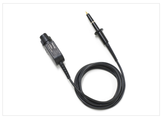
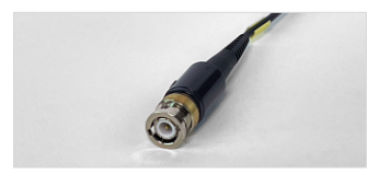
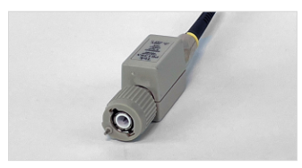
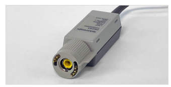
Such a probing system is shown in Figure 2.2a. These probes, however, are too small for practical use in applications such as industrial power circuitry where high voltages and larger gauge wires are common. For power applications, physically larger probes with greater margins of safety are required. Figures 2.2b and 2.2c show examples of such probes, where Figure 2.2b is a high-voltage probe and Figure 2.2c is a clamp-on current probe.
Figure 2.2. Various probes are available for different application technologies and measurement needs.
From these few examples of physical connection, it’s clear that there’s no single ideal probe size or configuration for all applications. Because of this, various probe sizes and configurations have been designed to meet the physical connection requirements of various applications.
Absolute Signal Fidelity
The ideal probe should transmit any signal from probe tip to oscilloscope input with absolute signal fidelity. In other words, the signal as it occurs at the probe tip should be faithfully duplicated at the oscilloscope input.
For absolute fidelity, the probe circuitry from tip to oscilloscope input must have zero attenuation, infinite bandwidth, and linear phase across all frequencies. Not only are these ideal requirements impossible to achieve in reality, but they are impractical. For example, there’s no need for an infinite bandwidth probe or oscilloscope when dealing with audio frequency signals. In addition, there is no need for infinite bandwidth when 500 MHz is sufficient for covering most high-speed digital, TV, and other typical oscilloscope applications.
Still, within a given bandwidth of operation, absolute signal fidelity is an ideal to be sought after.
Zero Signal Source Loading
The circuitry behind a test point can be thought of as or modeled as a signal source. Any external device, such as a probe, that’s attached to the test point can appear as an additional load on the signal source behind the test point.
The external device acts as a load when it draws signal current from the circuit (the signal source). This loading, or signal current draw, changes the operation of the circuitry behind the test point, and thus changes the signal seen at the test point.
An ideal probe causes zero signal source loading. In other words, it doesn’t draw any signal current from the signal source. This means that, for zero current draw, the probe must have infinite impedance, essentially presenting an open circuit to the test point.
In practice, a probe with zero signal source loading cannot be achieved. This is because a probe must draw some small amount of signal current in order to develop a signal voltage at the oscilloscope input. Consequently, some signal source loading is to be expected when using a probe. The goal, however, should always be to minimize the amount of loading by selecting the appropriate probe.
Complete Noise Immunity
Fluorescent lights and fan motors are just two of the many electrical noise sources in our environment. These sources can induce their noise onto nearby electrical cables and circuitry, causing the noise to be added to signals. Because of susceptibility to induced noise, a simple piece of wire is a less than ideal choice for an oscilloscope probe.
The ideal oscilloscope probe is completely immune to all noise sources. As a result, the signal delivered to the oscilloscope has no more noise on it than what appeared on the signal at the test point.
In practice, use of shielding allows probes to achieve a high level of noise immunity for most common signal levels. Noise, however, can still be a problem for certain low-level signals. In particular, common mode noise can present a problem for differential measurements, as will be discussed later.
The Realities of Probes
The preceding discussion of The Ideal Probe mentioned several realities that keep practical probes from reaching the ideal. To understand how this can affect your oscilloscope measurements, we need to explore the realities of probes further.
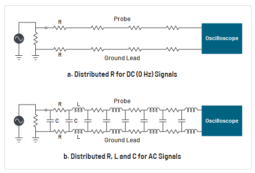
First, it’s important to realize that a probe, even if it’s just a simple piece of wire, is potentially a very complex circuit. For DC signals (0 Hz frequency), a probe appears as a simple conductor pair with some series resistance and a terminating resistance (Figure 2.3a). However, for AC signals, the picture changes dramatically as signal frequencies increase (Figure 2.3b).
The picture changes for AC signals because any piece of wire has distributed inductance (L), and any wire pair has distributed capacitance (C). The distributed inductance reacts to AC signals by increasingly impeding AC current flow as signal frequency increases. The distributed capacitance reacts to AC signals with decreasing impedance to AC current flow as signal frequency increases. The interaction of these reactive elements (L and C), along with the resistive elements (R), produces a total probe impedance that varies with signal frequency. Through good probe design, the R, L, and C elements of a probe can be controlled to provide desired degrees of signal fidelity, attenuation, and source loading over specified frequency ranges. Even with good design, probes are limited by the nature of their circuitry. It’s important to be aware of these limitations and their effects when selecting and using probes.
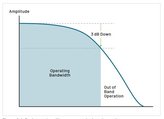
Bandwidth and Rise Time Limitations
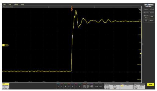
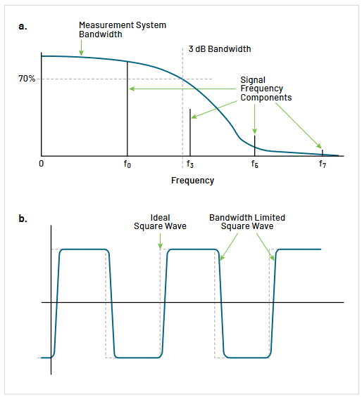
Bandwidth is the range of frequencies that an oscilloscope or probe is designed for. For example, a 100 MHz probe or oscilloscope is designed to make measurements within specification on all frequencies up to 100 MHz. Unwanted or unpredictable measurement results can occur at signal frequencies above the specified bandwidth (Figure 2.4). As a general rule, for accurate amplitude measurements, the bandwidth of the oscilloscope should be three to five times greater than the frequency of the waveform being measured. This improves the accuracy of amplitude measurements by staying clear of the 3 dB attenuation frequency as shown in Figure 2.4. For a system with a first order (Gaussian) rolloff, the measured amplitude at the -3 dB point is about 70% of the actual amplitude. Some high-performance oscilloscopes and probes have a steeper rolloff, and will produce more accurate amplitude measurements closer to their rated bandwidth. Using a probe/scope combination with five times the bandwidth of the frequency of your signal will deliver accurate amplitude measurements without concern.
It is also important to remember that the graph in Figure 2.4 applies to pure sinewaves. The maximum frequency components of square waves and pulses are harmonics of the fundamental frequency of the signal. To get an accurate view of a square wave, one must be able to see the fifth harmonic or even the seventh.
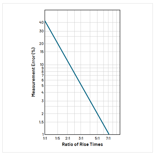
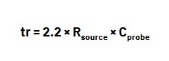
Similarly, the oscilloscope must have an adequate rise time for the waveforms being measured. The rise time of an oscilloscope or probe is defined as the time it takes the pulse to rise from the 10% amplitude level to the 90% amplitude level. For reasonable accuracy in measuring pulse rise or fall times, the rise time of the probe and oscilloscope together should be three to five times faster than that of the pulse being measured (Figure 2.5).
Every oscilloscope has defined bandwidth and rise time limits. Similarly, every probe also has its own set of bandwidth and rise time limits. When a probe is attached to an oscilloscope, you get a new set of system bandwidth and rise time limits.
Unfortunately, the relationship between system bandwidth and the individual oscilloscope and probe bandwidths is not a simple one. The same is true for rise times. To cope with this, manufacturers of quality oscilloscopes specify bandwidth or rise time to the probe tip when the oscilloscope is used with specific probe models. This is important because the oscilloscope and probe together form a measurement system, and it’s the bandwidth and rise time of the system that determine its measurement capabilities. If you use a probe that is not on the oscilloscope’s recommended list of probes, you run the risk of unpredictable measurement results.
Dynamic Range Limitations
All probes have a high-voltage safety limit that should not be exceeded. For passive probes, this limit can range from hundreds of volts to thousands of volts. However, for active probes, the maximum safe voltage limit is often in the range of tens of volts. To avoid personal safety hazards, as well as potential damage to the probe, it’s wise to be aware of the voltages being measured and the voltage limits of the probes being used.
In addition to safety considerations, there’s also the practical consideration of measurement dynamic range. Oscilloscopes have amplitude sensitivity ranges. For example, 1 mV to 10 V/division is a typical sensitivity range. On an eight-division display, this means that you can typically make reasonably accurate measurements on signals ranging from 4 mV peak-to-peak to 40 V peak-to-peak.
This assumes, at minimum, a four-division amplitude display of the signal to obtain reasonable measurement resolution. With a 1X probe (1-times probe), the dynamic measurement range is the same as that of the oscilloscope. For the example above, this would be a signal measurement range of 4 mV to 40 V.
With a 1X probe (1-times probe), the dynamic measurement range is the same as that of the oscilloscope. For the example above, this would be a signal measurement range of 4 mV to 40 V.
But, what if you need to measure a signal beyond the 40 V range?
You can shift the oscilloscope’s dynamic range to higher voltages by using an attenuating probe. A 10X probe, for example, shifts the dynamic range to 40 mV to 400 V. It does this by attenuating the input signal by a factor of 10, which effectively multiplies the oscilloscope’s scaling by 10. For most general-purpose use, 10X probes are preferred, both because of their high-end voltage range and because they cause less signal source loading. However, if you plan to measure a very wide range of voltage levels, you may want to complement the 10X probe with a 1X probe. This combination gives you a dynamic range of 4 mV to 400 V. However, in the 1X mode, more care must be taken with regard to signal source loading.
Source Loading
As previously mentioned, a probe must draw some signal current in order to develop a signal voltage at the oscilloscope input. This places a load at the test point that can change the signal that the circuit, or signal source, delivers to the test point.
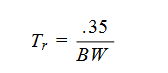
The simplest example of source loading effects is to consider measurement of a battery-driven resistive network. This is shown in Figure 2.7. In Figure 2.7a, before a probe is attached, the battery’s DC voltage is divided across the battery’s internal resistance (Ri) and the load resistance
(Ri) that the battery is driving. For the values given in the diagram, this results in an output voltage of:
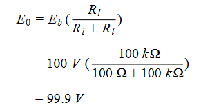
In Figure 2.7b, a probe has been attached to the circuit, placing the probe resistance (Rp) in parallel with RI . If Rp is 100 kΩ, the effective load resistance in Figure 2.7b is cut in half to 50 kΩ.
The loading effect of this on Eo is:
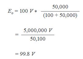
This loading effect of 99.9 V versus 99.8 V is only 0.1% and is negligible for most purposes. However, if the resistance of the probe (Rp) were smaller, say 10 kΩ, the effect would no longer be negligible.
To minimize such resistive loading, 1X probes typically have a resistance of 1 MΩ, and 10X probes typically have a resistance of 10 MΩ. For most cases, these values result in negligible resistive loading. Some loading should be expected, though, when measuring high-resistance sources.
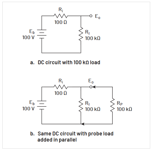
Usually, the loading of greatest concern is that caused by the capacitance at the probe tip (see Figure 2.8). For low frequencies, this capacitance has a reactance that is very high, and there’s little or no effect. But, as frequency increases, the capacitive reactance decreases. The result is increased loading at high frequencies.
This capacitive loading affects the bandwidth and rise time characteristics of the measurement system by reducing bandwidth and increasing rise time.
Capacitive loading can be minimized by selecting probes with low tip capacitance values. Some typical capacitance values for various probes are provided in the table below:
| Probe | Attenuation | R | C |
| P6101B | 1X | 1 MΩ | 100 pF |
| P6139B | 10X | 10 MΩ | 8 pF |
| P6243 | 10X | 1 MΩ | ≤1 pF |
| TPP1000 | 10X | 10 MΩ | 12 pF |
Table 1.1. Probe capacitance.
Since the ground lead is a wire, it has some amount of distributed inductance (see Figure 2.9). This inductance interacts with the probe capacitance to cause ringing at a certain frequency that is determined by the L and C values. This ringing is unavoidable, and may be seen as a sinusoid of decaying amplitude that is impressed on pulses. The effects of ringing can be reduced by designing probe grounding so that the ringing frequency occurs beyond the bandwidth limit of the probe/oscilloscope system.
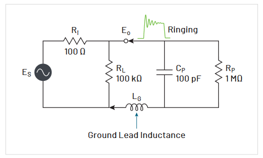
To avoid grounding problems, always use the shortest ground lead provided with the probe. Substituting other means of grounding can cause ringing to appear on measured pulses.
Probes are Sensors
In dealing with the realities of oscilloscope probes, it’s important to keep in mind that probes are sensors. Most oscilloscope probes are voltage sensors. That is, they sense or probe a voltage signal and convey that voltage signal to the oscilloscope input. However, there are also probes that allow you to sense phenomena other than voltage signals.
For example, current probes are designed to sense the current flowing through a wire. The probe converts the sensed current to a corresponding voltage signal which is then relayed to the input of the oscilloscope. Similarly, optical probes sense light power and convert it to a voltage signal for measurement by an oscilloscope.
Additionally, oscilloscope voltage probes can be used with a variety of other sensors or transducers to measure different phenomena. A vibration transducer, for example, allows you to view machinery vibration signatures on an oscilloscope screen. The possibilities are as wide as the variety of available transducers on the market.
In all cases, though, the transducer, probe, and oscilloscope combination must be viewed as a measurement system. Moreover, the realities of probes discussed above also extend down to the transducer. Transducers have bandwidth limits as well and can cause loading effects.
Some Probing Tips
Selecting probes that match your oscilloscope and application needs gives you the capability for making the necessary measurements. Actually making the measurements and obtaining useful results also depends on how you use the tools. The following probing tips will help you avoid some common measurement pitfalls:
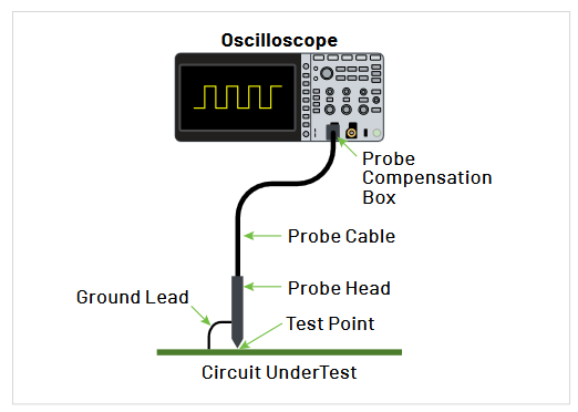
Compensate Your Probes
Most probes are designed to match the inputs of specific oscilloscope models. However, there are slight variations from oscilloscope to oscilloscope, and even between different input channels in the same oscilloscope. To deal with this where necessary, many probes, especially attenuating probes (10X and 100X probes), have built-in compensation networks.
If your probe has a compensation network, you should adjust this network to compensate the probe for the oscilloscope channel that you are using. To do this, use the following procedure:
For Probes Requiring Manual Compensation:
- Attach the probe to the oscilloscope.
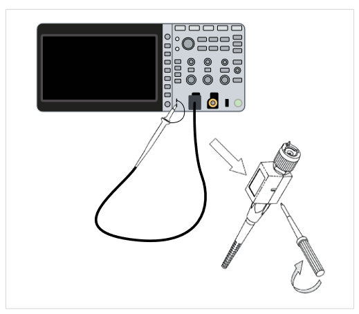
- Attach the probe tip to the probe compensation test point on the oscilloscope’s front panel (see Figure 2.10).
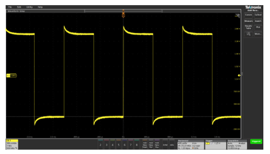
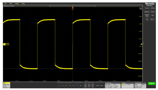
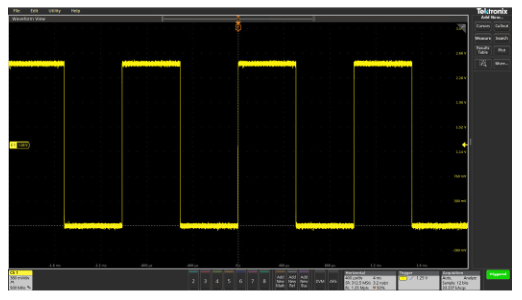
- Use the adjustment tool provided with the probe or other non-magnetic adjustment tool to adjust the compensation network to obtain a calibration waveform display that has flat tops with no overshoot or rounding (see Figure 2.12).
- If the oscilloscope has a built-in calibration routine, run this routine for increased accuracy.
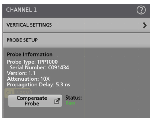
For Modern Probes with Automatic Digital Compensation:
- Attach the probe to the oscilloscope.
- Attach probe tip to the compensation test point on the oscilloscope’s front panel (see Figure 2.10).
- Click the ‘autoset’ button on the front of the oscilloscope.
- Double tap or double click the channel badge in the bottom left corner of the screen.
- Navigate to the ‘probe setup’ drop down menu.
- Tap or click the ‘compensate probe’ button (see Figure 2.11).
An uncompensated probe can lead to various measurement errors, especially in measuring pulse rise or fall times. To avoid such errors, always compensate probes right after connecting them to the oscilloscope and check compensation frequently.
Also, it’s wise to check probe compensation whenever you change probe tip adaptors. Some modern oscilloscope “remember” the compensation for specific probes, such as TekVPI probes. For these systems probe compensation can simply be verified with a quick test.
Figure 2.12. Examples of probe compensation effects on a square wave.
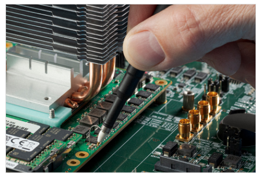
Use Appropriate Probe Tip Adapters Whenever Possible
A probe tip adapter that’s appropriate for the circuit being measured makes probe connection quick, convenient, and electrically repeatable and stable. Unfortunately, it’s not uncommon to see short lengths of wire soldered to circuit points as a substitute for a probe tip adapter.
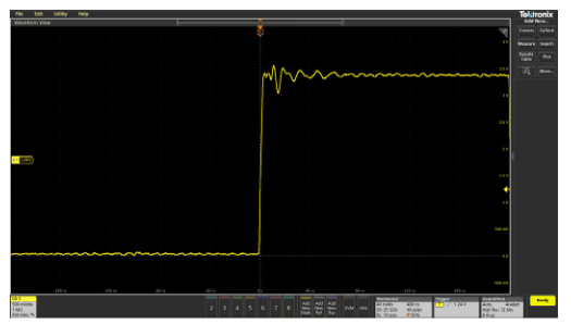
The problem is that even an inch or two of wire can cause significant impedance changes at high frequencies. The effect of this is shown in Figure 2.13, where a circuit is measured by direct contact of the probe tip and then measured via a short piece of wire between the circuit and probe tip.
Figure 2.13. Even a short piece of wire soldered to a test point can cause signal fidelity problems. In this case, rise time has been changed from 4.74 ns to 5.67 ns.
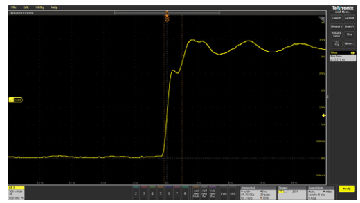
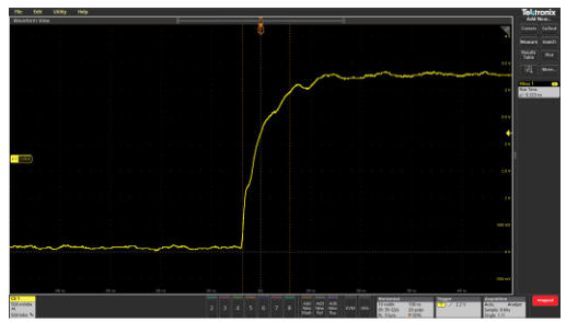
Keep Ground Leads as Short and as Direct as Possible
When doing performance checks or troubleshooting large boards or systems, it may be tempting to extend the probe’s ground lead. An extended ground lead allows you to attach the ground once and freely move the probe around the system while you look at various test points. However, the added inductance of an extended ground lead can cause ringing to appear on fast-transition waveforms. This is illustrated in Figure 2.14, which shows waveform measurements made while using the standard probe ground lead and an extended ground lead.
Figure 2.14. Extending the length of the probe ground lead can cause ringing to appear on pulses.
Summary
In this first chapter, we’ve tried to provide all of the basic information necessary for making appropriate probe selections and using probes properly. In the following chapters, we’ll expand on this information as well as introduce more advanced information on probes and probing techniques.
3. Different Probes for Different Needs
Hundreds, perhaps even thousands, of different oscilloscope probes are available on the market.
Is such a broad selection of probes really necessary? The answer is yes, and in this chapter you’ll discover the reasons why
With an understanding of those reasons, you’ll be better prepared to make probe selections to match both the oscilloscope you are using and the type of measurements that you need to make. The benefit is that proper probe selection leads to enhanced measurement capabilities and results.
Why So Many Probes?
The wide selection of oscilloscope models and capabilities is one of the fundamental reasons for the number of available probes. Different oscilloscopes require different probes. A 400 MHz oscilloscope requires probes that will support that 400 MHz bandwidth.
However, those same probes would be overkill in capability and cost for a 100 MHz oscilloscope. Thus, a different set of probes designed to support a 100 MHz bandwidth is needed.
As a general rule, probes should be selected to match the oscilloscope’s bandwidth whenever possible. If matching the oscilloscope’s bandwidth isn’t a possibility, choose to exceed the oscilloscope’s bandwidth.
Bandwidth is just the beginning, though. Oscilloscopes can also have different input connector types and different input impedances. For example, most scopes use a simple BNC-type input connector. Others may use an SMA connector. And still others, as shown in Figure 3.1, have specially designed connectors to support readout, trace ID, probe power, or other special features.
Thus, probe selection must also include connector compatibility with the oscilloscope being used. This can be direct connector compatibility, or connection through an appropriate adaptor.
Figure 3.1. Probe to oscilloscope interfaces
 |
 |
 |
 |
 |
|
|
|
|
|
|
Readout support is a particularly important aspect of probe/oscilloscope connector compatibility. When 1X and 10X probes are interchanged on an oscilloscope, the oscilloscope’s vertical scale readout should reflect the 1X to 10X change. For example, if the oscilloscope’s vertical scale readout is 1 V/div (one volt per division) with a 1X probe attached, and you change to a 10X probe, the vertical readout should change by a factor of 10 to 10 V/div. If this 1X to 10X change is not reflected in the oscilloscope’s readout, amplitude measurements made with the 10X probe will be ten times lower than they should be.
Some generic or commodity probes may not support readout capability for all scopes. As a result, extra caution is necessary when using generic probes in place of the probes specifically recommended by the oscilloscope manufacturer.
In addition to bandwidth and connector differences, various scopes also have different input resistance and capacitance values. Typically, oscilloscope input resistances are either 50 Ω or 1 MΩ. However, there can be great variations in input capacitance depending on the oscilloscope’s bandwidth specification and other design factors. For proper signal transfer and fidelity, it’s important that the probe’s resistance and capacitance values match the resistance and capacitance values of the oscilloscope it is to be used with. For example, 50 Ω probes should be used with 50 Ω oscilloscope inputs. Similarly, 1 MΩ probes should be used on scopes with a 1 MΩ input resistance.
An exception to this one-to-one resistance matching occurs when attenuator probes are used. For example, a 10X probe for a 50 Ω environment will have a 500 Ω input resistance, and a 10X probe for a 1 MΩ environment will have a 10 MΩ input resistance. (Attenuator probes, such as a 10X probe, are also referred to as divider probes and multiplier probes. These probes multiply the measurement range of the oscilloscope. They do this by attenuating or dividing down the input signal supplied to the oscilloscope.)
In addition to resistance matching, the probe’s capacitance should also match the nominal input capacitance of the oscilloscope. Often, this capacitance matching can be done through adjustment of the probe’s compensation network. This is only possible, though, when the oscilloscope’s nominal input capacitance is within the compensation range of the probe. Thus, it’s not unusual to find probes with different compensation ranges to meet the requirements of different oscilloscope inputs.
The issue of matching a probe to an oscilloscope has been tremendously simplified by oscilloscope manufacturers. Oscilloscope manufacturers carefully design probes and oscilloscopes as complete systems. As a result, the best probe-to-oscilloscope match is always obtained by using the standard probe specified by the oscilloscope manufacturer. Use of any probe other than the manufacturer-specified probe may result in less than optimum measurement performance.
Probe-to-oscilloscope matching requirements alone generate much of the basic probe inventory available on the market. This probe count is then added to significantly by the different probes that are necessary for different measurements needs. The most basic differences are in the voltage ranges being measured. Millivolt, volt, and kilovolt measurements typically require probes with different attenuation factors (1X, 10X, 100X).
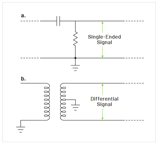
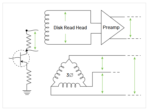
Also, there are many cases where the signal voltages are differential. That is, the signal exists across two points or two wires, neither of which is at ground or common potential (see Figure 3.2). Such differential signals are common in amplifier circuits, serial data communications, and power circuits. Measuring these signals requires yet another class of probes referred to as differential probes.
There are many cases, particularly in power applications, where current is of as much or more interest than voltage. Such applications are best served with yet another class of probes that sense current rather than voltage.
Current probes and differential probes are just two special classes of probes among the many different types of available probes. The rest of this chapter covers some of the more common types of probes and their special benefits.
Different Probe Types and Their Benefits
As a preface to discussing various common probe types, it’s important to realize that there’s often overlap in types. Certainly a voltage probe senses voltage exclusively, but a voltage probe can be a passive probe, or an active probe. Similarly, differential probes are a special type of voltage probe, and differential probes can also be active or passive probes. These overlapping relationships will be pointed out where appropriate.
Passive Voltage Probes
Passive probes are constructed of wires and connectors — and when needed for compensation or attenuation — also contain resistors and capacitors. There are no active components (transistors or amplifiers) in the probe’s signal path.
Because of their relative simplicity, passive probes tend to be the most rugged and economical of probes. They are easy to use and are also the most widely used type of probe.
Passive voltage probes are available with various attenuation factors – 1X, 10X, and 100X – for different voltage ranges. Of these, the 10X passive voltage probe is the most commonly used, and is the type of probe typically supplied as a standard accessory with oscilloscopes.
For applications where signal amplitudes are one-volt peak-to-peak or less, a 1X probe may be more appropriate, or even necessary. Where there’s a mix of low amplitude and moderate amplitude signals (tens of millivolts to tens of volts), a switchable 1X/10X probe can be a great convenience. It should be kept in mind, however, that a switchable 1X/10X probe is essentially two different probes in one. Not only are their attenuation factors different, but their bandwidth, rise time, and impedance (R and C) characteristics are different as well. As a result, these probes will not exactly match the oscilloscope’s input and will not provide the optimum performance achieved with a standard 10X probe.
Most passive probes are designed for use with general purpose oscilloscopes. As such, their bandwidths typically range from less than 100 MHz to 500 MHz or more.
A wide range of accessories are available for these probes,to facilitate connection to different wires, components or test points. See “Probe Accessories” and Figure 3.17 later in this chapter.
There is, however, a special category of passive probes that provide much higher bandwidths. They are referred to variously as 50 Ω probes, Zo probes, and voltage divider probes. These probes are designed for use in 50 Ω environments, which typically are high-speed device characterization, microwave communication, and time domain reflectometry (TDR). A typical 50 Ω probe for such applications has a bandwidth of several gigaHertz and a rise time of 100 picoseconds or faster.
Single Ended Active Voltage Probes
Active probes contain or rely on active components, such as transistors, for their operation. Most often, the active device is a field-effect transistor (FET).
The advantage of a FET input is that it provides a very low input capacitance, typically a few picoFarads (pF) down to less than 1 pF. Such ultra-low capacitance has several desirable effects.
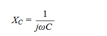
First, recall that a low value of capacitance, C, translates to a high value of capacitive reactance, Xc. This can be seen from the formula for Xc, which is:
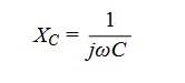
Since capacitive reactance is the primary input impedance element of a probe, a low C results in a high input impedance over a broader band of frequencies. As a result, active FET probes will typically have specified bandwidths ranging from 500 MHz to several GHz
In addition to higher bandwidth, the high input impedance of active FET probes allows measurements at test points of unknown impedance with much less risk of loading effects. Also, longer ground leads can be used since the low capacitance reduces ground lead effects. The most important aspect, however, is that FET probes offer such low loading, that they can be used on high-impedance circuits that would be considerably loaded by passive probes.
With all of these positive benefits, including bandwidths as wide as DC to several GHz, you might wonder: Why bother with passive probes?
The answer is that active FET probes don’t have the voltage range of passive probes. The linear dynamic range of active probes is generally anywhere from ±0.6 V to ±10 V. In addition, the maximum voltage that they can withstand can be as low as ±40 V (DC + peak AC). In other words, you can’t measure from millivolts to tens of volts like you can with a passive probe. In addition, active probes can be damaged by inadvertently probing a higher voltage. They can even be damage by a static discharge.
Still, the high bandwidth of FET probes is a major benefit and their linear voltage range covers many typical semiconductor voltages. Thus, active FET probes are often used for low signal level applications, including fast logic families such as ECL, GaAs, and others.
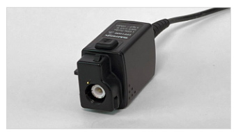
Power Rail Probes
Traditional power integrity applications typically use passive or differential probes to measure power rails. With the changing technology landscape, designers need higher accuracy ripple measurements with very fast transitions pushing into multiple GHz range. New design challenges call for new probing techniques that can minimize noise from the measurement tools while also offering more bandwidth to see more signal content. A power rail probe is built for such a purpose and offers low loading for accuracy (especially in the most sensitive measurements) and offers low noise contribution and high bandwidth options. The higher bandwidth helps to see more signal content (harmonics, faster ripples, etc.) on DC rails that could affect data signals, and clocks.
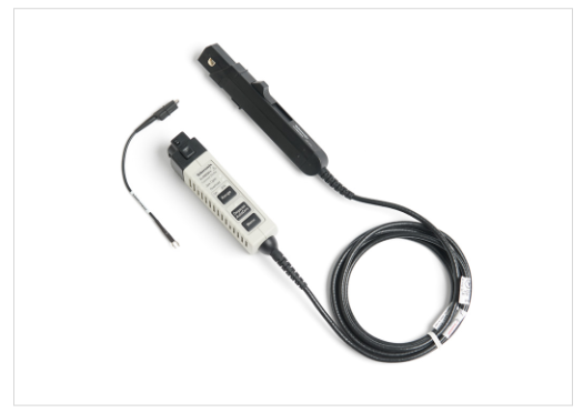
An example of such a probe is shown in Figure 3.3.
The power rail probe covers power rail transient events up to several GHz and offers a large DC offset voltage range of 10s of volts to measure power supplies from plug, down to the pin of an integrated circuit. It also supports a wide dynamic range for power integrity applications, which, on higher voltage rails, lets the user look at droop on the line or when a lot of current is drawn by load or transients. The higher input impedance (50 kΩ at DC) in these probes minimize the oscilloscope loading effect on DC rails.
As the technology advances, power engineers are challenged to get more power efficiency from smaller and tighter designs. This is especially true for engineers in the automotive, industrial and consumer markets where typical validation requires probing at least one or more rails in parallel with other signals. This creates new constraints on connectivity due to tight spacing, buried signals, and smaller geometry components. The power rail probe comes with a modular and flexible connectivity options to cover most needs.
Differential Probes
Differential signals are signals that are referenced to each other instead of earth ground. Figure 3.4 illustrates several examples of such signals. These include the signal developed across a collector load resistor, high speed serial data signals, inverter output AC signals, multi-phase power systems, and numerous other situations where signals are in essence “floating” above ground. Some differential probes also come with ground cables. This isn’t necessary in all applications, but can help increase signal fidelity. If there is a lot of common mode noise, the ground cable
could be a better path for the noise to follow so it doesn’t pollute your measurements. Another reason to use this ground cable is for safety. When using differential probes, it is common that your test point could be floating hundreds of volts above ground. Adding a ground cable also protects against electrostatic discharge (ESD).
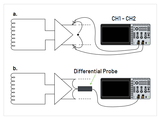
Differential signals can be probed and measured in two basic ways. Both approaches are illustrated in Figure 3.5.
Using two probes to make two single-ended measurements, as shown in Figure 3.5a is a commonly used method. It’s also usually the least desirable method of making differential measurements. Nonetheless, the method is often used because a dual-channel oscilloscope is available with two probes. Measuring both signals to ground (single-ended) and using the oscilloscope’s math functions to subtract one from the other (channel A signal minus channel B) seems like an elegant solution to obtaining the difference signal, and it can be in situations where the signals are low frequency and have enough amplitude to be above any concerns of noise.
There are several potential problems with combining two single-ended measurements. One problem is that there are two long and separate signal paths down each probe and through each oscilloscope channel. Any delay differences between these paths results in time skewing of the two signals. On high-speed signals, this skew can result in significant amplitude and timing errors in the computed difference signal. To minimize this, matched probes should be used.
Another problem with single-ended measurements is that they don’t provide adequate common-mode noise rejection. Common-mode noise is noise that is impressed on both signal lines by such things as nearby clock lines or noise from external sources such as fluorescent lights. Many low-level signals, such as disk read channel signals, are transmitted and processed differentially in order to take advantage of common-mode noise rejection. In a differential system this common-mode noise tends to be subtracted out of the differential signal. The success with which this is done is referred to as the common-mode rejection ratio (CMRR).
Because of channel differences, the CMRR performance of single-ended measurements quickly declines to dismal levels with increasing frequency. This results in the signal appearing noisier than it actually would be if the commonmode rejection of the source had been maintained.
A differential probe, on the other hand, uses a differential amplifier to subtract the two signals, resulting in one differential signal for measurement by one channel of the oscilloscope (Figure 3.5b).
This provides substantially higher CMRR performance over a broader frequency range. Additionally, advances in circuit miniaturization have allowed differential amplifiers to be moved down into the actual probe head. In modern differential voltage probes, it is possible to achieve 60 dB (1000:1) or more of common mode rejection at 1 MHz and 30 dB (32:1) or more at 1 GHz. Optically isolated probes deliver even higher CMRR.
High-voltage Probes
The term “high voltage” is relative. What is considered high voltage in the semiconductor industry is practically nothing in the power industry. From the perspective of probes, however, we can define high voltage as being any voltage beyond what can be handled safely with a typical, generalpurpose 10X passive probe.
Typically, the maximum voltage for general-purpose passive probes is around 400 to 500 volts (DC + peak AC). Highvoltage probes on the other hand can have maximum ratings as high as 20,000 volts. An example of a high-voltage probe is shown in Figure 3.6.
Safety is a particularly important aspect of high-voltage probes and measurements. To accommodate this, many high-voltage probes have longer than normal cables. Typical cable lengths are 10 feet. This is usually adequate for locating the oscilloscope outside of a safety cage or behind a safety shroud. Options for 25-foot cables are also available for those cases where oscilloscope operation needs to be further removed from the high-voltage source.
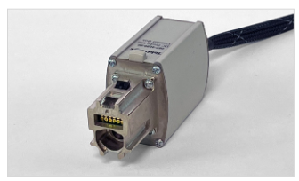
Optically Isolated Probes
An isolated probe uses galvanic isolation to isolate the reference voltage of the probe from the reference voltage of the oscilloscope (typically earth ground). Because there is no electrical connection between the device under test and the oscilloscope, common mode currents have no path through the instrument, resulting in very high common mode rejection ratio, even at bandwidths of 500 MHz or 1 GHz.
While a high-quality, traditional differential probe would offer CMRR of –25dB at 100 MHz, an optically isolated probe can offer –120 dB. Isolation can also enable high differential voltage ranges into the kilovolt range.
Tektronix has developed a patented technology (called IsoVu) that uses optical isolation to provide best in class common mode rejection performance across a wide bandwidth. The IsoVu technology uses power-over-fiber and an optical analog signal path for complete galvanic isolation between the measurement system and the DUT. This technology is very useful, especially for making accurate voltage measurements on power converters that use fastswitching wide bandgap semiconductors.
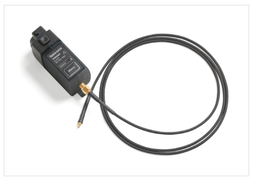
A Tektronix IsoVu probe is shown in Figure 3.7.
Floating Measurements
Floating measurements are measurements that are made between two points, neither of which is at ground potential. If this sounds a lot like differential measurements described previously with regard to differential probes, you’re right. A floating measurement is a differential measurement, and, in fact, floating measurements can be made using differential probes.
Generally, however, the term “floating measurement” is used in referring to power system measurements. Examples are switching supplies, motor drives, ballasts, and uninterruptible power sources where neither point of the measurement is at ground (earth potential). In addition, the signal “common” may be elevated (floating) to hundreds of volts from ground. Often, these measurements require rejection of high common-mode signals in order to evaluate low-level signals riding on them. Extraneous ground currents can also add hum to the display, causing even more measurement difficulty.
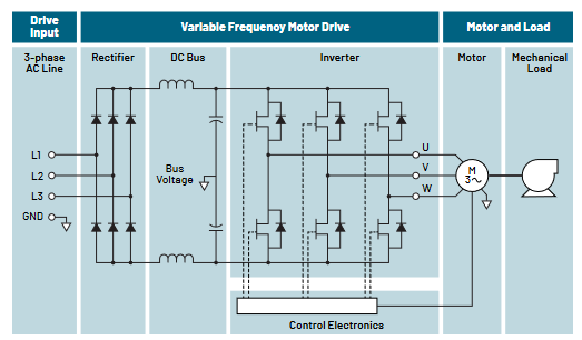
An example of a typical floating measurement situation is shown in Figure 3.8. In this motor drive system, the three phase AC line is rectified to a floating DC bus of up to 600 V. The ground-referenced control circuit generates pulse modulated gate drive signals through an isolated driver to the bridge transistors, causing each output to swing the full bus voltage at the pulse modulation frequency. Accurate measurement of the gate-to-source voltage requires rejection of the bus transitions. Additionally, the compact design of the motor drive, fast current transitions, and proximity to the rotating motor contribute to a harsh EMI environment.
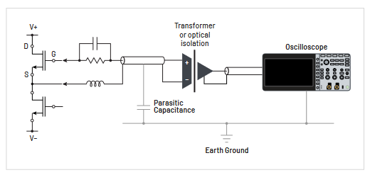
Also, connecting the ground lead of an oscilloscope’s probe to any part of the motor drive circuit would cause a short to ground.
Rather than floating the oscilloscope, the probe isolator floats just the probe. This isolation of the probe can be done via either a transformer or optical coupling mechanism, as shown in Figure 3.9. In this case, the oscilloscope remains grounded, as it should, and the differential signal is applied to the tip and reference lead of the isolated probe. The isolator transmits the differential signal through the isolator to a receiver, which produces a ground-referenced signal that is proportional to the differential input signal. This makes the probe isolator compatible with virtually any instrument.
To meet different needs, various types of isolators are available. These include multi-channel isolators that provide two or more channels with independent reference leads. Also, fiber-optic based isolators are available for cases where the isolator needs to be physically separated from the instrument by long distances (e.g. 100 meters or more). As with differential probes, the key isolator selection criteria are bandwidth and CMRR. Additionally, maximum working voltage is a key specification for isolation systems.
Caution
To get around this direct short to ground, some oscilloscope users have used the unsafe practice of defeating the oscilloscope’s ground circuit. This allows the oscilloscope’s ground lead to float with the motor drive circuit so that differential measurements can be made. Unfortunately, this practice also allows the oscilloscope chassis to float at potentials that could be a dangerous or deadly shock hazard to the oscilloscope user.
Not only is “floating” the oscilloscope an unsafe practice, but the resulting measurements are often impaired by noise and other effects.
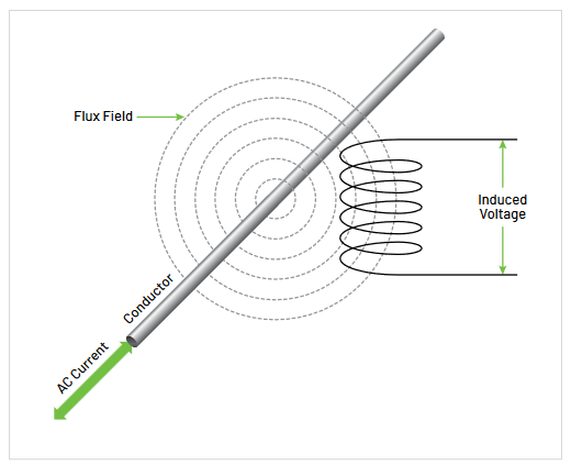
Current Probes
Current flow through a conductor causes an electromagnetic flux field to form around the conductor. Current probes are designed to sense the strength of this field and convert it to a corresponding voltage for measurement by an oscilloscope. This allows you to view and analyze current waveforms with an oscilloscope.
When used in combination with an oscilloscope’s voltage measurement capabilities, current probes also allow you to make a wide variety of power measurements. Depending on the waveform math capabilities of the oscilloscope, these measurements can include instantaneous power, true power, apparent power, and phase.
There are two types of current probes for oscilloscopes. AC current probes, which are usually passive probes, and AC/DC current probes, which are generally active probes. Both types use the same principle of transformer action for sensing alternating current (AC) in a conductor.
For transformer action, there must first be alternating current flow through a conductor. This alternating current causes a flux field to build and collapse according to the amplitude and direction of current flow. When a coil is placed in this field, as shown in Figure 3.10, the changing flux field induces a voltage across the coil through simple transformer action.
This transformer action is the basis for AC current probes. The AC current probe head is actually a coil that has been wound to precise specifications on a magnetic core. When this probe head is held within a specified orientation and proximity to an AC current carrying conductor, the probe outputs a linear voltage that is of known proportion to the current in the conductor. This current-related voltage can be displayed as a current-scaled waveform on an oscilloscope.
The bandwidth for AC current probes depends on the design of the probe’s coil and other factors. Bandwidths as high as a few GHz are possible. However, bandwidths under 100 MHz are more typical.
In all cases, there’s also a low-frequency cutoff for AC current probe bandwidth. This includes direct current (DC), since direct current doesn’t cause a changing flux field and, thus, cannot cause transformer action. Also at frequencies very close to DC, 0.01 Hz for example, the flux field still may not be changing fast enough for appreciable transformer action. Eventually, though, a low frequency is reached where the transformer action is sufficient to generate a measurable output within the bandwidth of the probe. Again, depending on the design of the probe’s coil, the lowfrequency end of the bandwidth might be as low as 0.5 Hz or as high as 1.2 kHz.
For probes with bandwidths that begin near DC, a Hall Effect device can be added to the probe design to detect DC. The result is an AC/DC probe with a bandwidth that starts at DC and extends to the specified upper frequency 3 dB point. This type of probe requires, at minimum, a power source for biasing the Hall Effect device used for DC sensing. Depending on the probe design, a current probe amplifier may also be required for combining and scaling the AC and DC levels to provide a single output waveform for viewing on an oscilloscope.
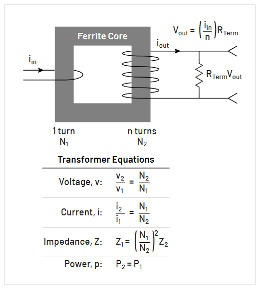
It’s important to keep in mind that a current probe operates in essence as a closely coupled transformer. This concept is illustrated in Figure 3.11, which includes the basic transformer equations. For standard operation, the sensed current conductor is a one-turn winding transformer (N1). The current from this single winding transforms to a multi-winding (N2) probe output voltage that is proportional to the turns ratio (N2/N1). At the same time, the probe’s impedance is transformed back to the conductor as a series insertion impedance. This insertion impedance is frequency dependent with its 1 MHz value typically being in the range of 30 to 500 mΩ, depending on the specific probe. The impedance appears in series within the circuit under test. For most cases, the small insertion impedance of a current probe imposes a negligible load.
Transformer basics can be taken advantage of to increase probe sensitivity by looping the conductor through the probe multiple times. Two loops doubles the sensitivity, and three loops triples the sensitivity. However, this also increases the insertion impedance by the square of the added turns.
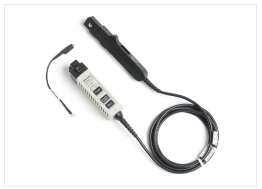
Figure 3.12 illustrates a particular class of probe referred to as a split core probe. The windings of this type of probe are on a “U” shaped core that is completed with a ferrite slide that closes the top of the “U”. The advantage of this type of probe is that the ferrite slide can be retracted to allow the probe to be conveniently clipped onto the conductor whose current is to be measured. When the measurement is completed the slide can be retracted and the probe can be moved to another conductor.
Probes are also available with solid-core current transformers. These transformers completely encircle the conductor being measured. As a result, they must be installed by disconnecting the conductor to be measured, feeding the conductor through the transformer, and then reconnecting the conductor to its circuit. The chief advantages of solid-core probes is that they offer small size and very high frequency response for measuring very fast, low amplitude current pulses and AC signals.
Split-core current probes are by far the most common type. These are available in both AC and AC/DC versions, and there are various current-per-division display ranges, depending on the amp-second product.
The amp-second product defines the maximum limit for linear operation of any current probe. This product is defined for current pulses as the average current amplitude multiplied by the pulse width. When the amp-second product is exceeded, the core material of the probe’s coil goes into saturation. Since a saturated core cannot handle any more current-induced flux, there can no longer be constant proportionality between current input and voltage output.
The result is that waveform peaks are essentially “clipped off” in areas where the amp-second product is exceeded.
Core saturation can also be caused by high levels of direct current through the conductor being sensed. To combat core saturation and effectively extend the current measuring range, some active current probes provide a bucking current. The bucking current is set by sensing the current level in the conductor under test and then feeding an equal but opposite current back through the probe. Because opposing currents are subtractive, the bucking current can be adjusted to keep the core from going into saturation.
Because of the wide range of current measuring needs from milliamps to kiloamps, and from DC to high frequencies, there’s a correspondingly wide selection of current probes. Choosing a current probe for a particular application is similar in many respects to selecting voltage probes. Important selection criteria include:
- Current handling capability
- Ranges and sensitivities
- Insertion impedance
- Frequency range and derating
- Maximum amp-second product
- Connectivity
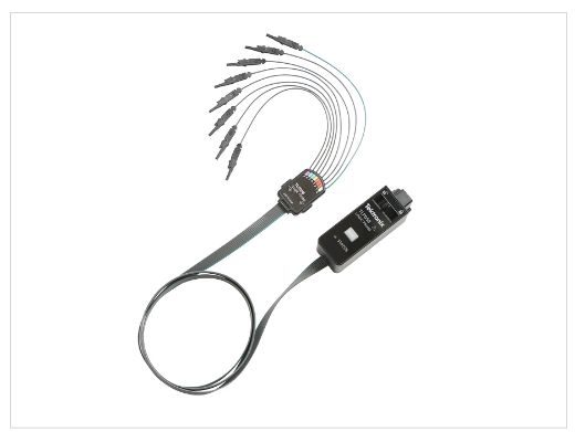
Logic Probes
Faults in digital systems can occur for a variety of reasons. While a logic analyzer is the traditional tool for identifying and isolating fault occurrences, the actual cause of the logic fault is often due to the analog attributes of the digital waveform. Pulse width jitter, pulse amplitude aberrations, and regular old analog noise and crosstalk are but a few of the many possible analog causes of digital faults.
Analyzing the analog attributes of digital waveforms requires use of an oscilloscope. However, to isolate exact causes, digital designers often need to look at specific data pulses occurring during specific logic conditions. Logic triggering and timing analysis can be added to mixed signal oscilloscopes through the use of a digital probe.
The logic probe shown in Figure 3.13 offers an eightchannel pod. Each channel ends with a probe tip featuring a recessed ground for simplified connection to the deviceunder-test. The coax on the first channel is colored blue, making it easy to identify. The common ground is accessible on two 0.187 inch quick connect tabs, making it easy to create custom grounds for connecting to the device-undertest using widely-available quick connect receptacles. When connecting to square pins, you can use an adapter that attaches to the probe head extending the probe ground flush with the probe tip so you can attach to a header. These probes offer outstanding electrical characteristics with minimal capacitive loading.
Optical Probes
With the advent and spread of fiber-optic based communications, there’s a rapidly expanding need for viewing and analyzing optical waveforms. A variety of specialized optical system analyzers have been developed to fill the needs of communication system troubleshooting and analysis. However, there’s also an expanding need for general-purpose optical waveform measurement and analysis during optical component development and verification. Optical probes fill this need by allowing optical signals to be viewed on an oscilloscope.
The optical probe is an optical-to-electrical converter. On the optical side, the probe must be selected to match the specific optical connector and fiber type or optical mode of the device that’s being measured. On the electrical side, the standard probe-to-oscilloscope matching criteria are followed.
Other Probe Types
In addition to all of the above “fairly standard” probe types, there’s also a variety of specialty probes and probing systems. These include:
- Environmental probes, which are designed to operate over a very wide temperature range.
- Temperature probes, which are used to measure the temperature of components and other heat generating items.
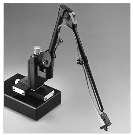
- Probing stations and articulated arms (Figure 3.14) for probing fine-pitch devices such as multi-chip-modules, hybrid circuits, and ICs.
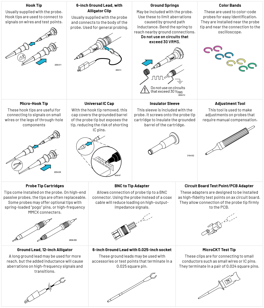
Probe Accessories
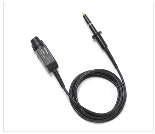
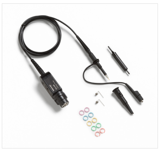
Most probes come with a package of standard accessories. These accessories often include a ground lead clip that attaches to the probe, and one or more probe tip accessories to aid in attaching the probe to various test points. Probes will often come with a probe compensation tool; however, some modern probes don’t require compensation by hand, and instead implement automatic digital compensation. Figure 3.15 shows an example of a typical general purpose voltage probe and its standard accessories.
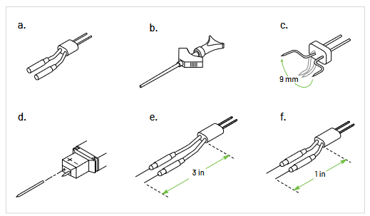
Probes that are designed for specific application areas, such as probing surface mount devices, may include additional probe tip adapters in their standard accessories package. Also, various special purpose accessories may be available as options for the probe. Figure 3.16 illustrates several types of probe tip adaptors designed for use with small geometry probes.
It’s important to realize that most probe accessories, especially probe tip adaptors, are designed to work with specific probe models. Switching adaptors between probe models or probe manufacturers is not recommended since it can result in poor connection to the test point or damage to either the probe or probe adaptor.
When selecting probes for purchase, it’s also important to take into account the type of circuitry that you’ll be probing and any adaptors or accessories that will make probing quicker and easier. In many cases, less expensive commodity probes don’t provide a selection of adaptor options. On the other hand, probes obtained through an oscilloscope manufacturer often have an extremely broad selection of accessories for adapting the probe to special needs. An example of this is shown in Figure 3.17, which illustrates the variety of accessories and options available for a particular class of probes. These accessories and options will, of course, vary between different probe classes and models.
4. A Guide to Probe Selection
The preceding chapters have covered a wide range of topics regarding oscilloscope probes in terms of how probes function, the various types of probes, and their effects on measurements. For the most part, the focus has been on what happens when you connect a probe to a test point.
In this chapter, the focus changes to the signal source and how to translate its properties into criteria for appropriate probe selection.
The goal, as always, is to select the probe that delivers the best representation of the signal to the oscilloscope. However, it doesn’t stop there. The oscilloscope imposes certain requirements that must also be considered as part of the probe selection process.
This chapter explores the various selection requirements, beginning with understanding the requirements imposed by the signal source.
Choosing the Right Probe
Because of the wide range of oscilloscope measurement applications and needs, there’s also a broad selection of oscilloscope probes on the market. This can make probe selection a confusing process.
To cut through much of the confusion and narrow the selection process, always follow the oscilloscope manufacturer’s recommendations for probes. This is important because different oscilloscopes are designed for different bandwidth, rise time, sensitivity, and input impedance considerations. Taking full advantage of the oscilloscope’s measurement capabilities requires a probe that matches the oscilloscope’s design considerations.
Additionally, the probe selection process should include consideration of your measurement needs. What are you trying to measure? Voltages? Current? An optical signal? By selecting a probe that is appropriate to your signal type, you can get direct measurement results faster.
Also, consider the amplitudes of the signals you are measuring. Are they within the dynamic range of your oscilloscope? If not, you’ll need to select a probe that can adjust dynamic range. Generally, this will be through attenuation with a 10X or higher probe.
Make sure that the bandwidth, or rise time, at the probe tip exceeds the signal frequencies or rise times that you plan to measure. Always keep in mind that non-sinusoidal signals have important frequency components or harmonics that extend well above the fundamental frequency of the signal. For example, to fully include the 5th harmonic of a 100 MHz square wave, you need a measurement system with a bandwidth of 500 MHz at the probe tip. Similarly, your oscilloscope system’s rise time should be three to five times faster than the signal rise times that you plan to measure.
In addition, always take into account possible signal loading by the probe. Look for high-resistance, low-capacitance probes. For most applications, a 10 MΩ probe with 20 pF or less capacitance should provide ample insurance against signal source loading. However, for some high-speed digital circuits you may need to move to the lower tip capacitance offered by active probes.
Finally, keep in mind that you must be able to attach the probe to the circuit before you can make a measurement. This may require special selection considerations about probe head size and probe tip adaptors to allow for easy and convenient circuit attachment.
Visit www.tek.com/probe-selector to find the recommended Tektronix probe for your testing needs.
Understanding the Signal Source
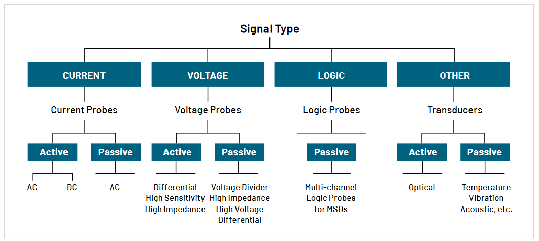
There are four fundamental signal source issues to be considered in selecting a probe. These are the signal type, the signal frequency content, the source impedance, and the physical attributes of the test point. Each of these issues is covered in the following discussion.
Signal Type
The first step in probe selection is to assess the type of signal to be probed. For this purpose, signals can be categorized as being one of the following:
- Voltage Signals
- Current Signals
- Logic Signals
- Other Signals
Voltage signals are the most commonly encountered signal type in electronic measurements. As such, voltage sensing probes are the most common type of oscilloscope probe. It should also be noted that since oscilloscopes require a voltage signal at their input, other types of oscilloscope probes are, in essence, transducers that convert the sensed phenomenon to a corresponding voltage signal. A common example of this is the current probe, which transforms a current signal into a voltage signal for viewing on an oscilloscope.
Logic signals are actually a special category of voltage signals. Logic probes for mixed signal oscilloscopes (MSOs) determine logic levels by comparing the input signals to adjustable voltage thresholds. The resulting high and low levels can be displayed on the MSO, and may also be used for triggering on specific binary combinations.
In addition to voltage, current, and logic signals, there are numerous other types of signals that may be of interest. These can include signals from optical, mechanical, thermal, acoustic, and other sources. Various transducers can be used to convert such signals to corresponding voltage signals for oscilloscope display and measurement.
Figure 4.1 provides a graphical categorization of probes based on the type of signal to be measured. Notice that under each category there are various probe subcategories that are further determined by additional signal attributes as well as oscilloscope requirements.
Signal Frequency Content
All signals, regardless of their type, have frequency content. DC signals have a frequency of 0 Hz, and pure sinusoids have a single frequency — that is the reciprocal of the sinusoid’s period. All other signals contain multiple frequencies whose values depend upon the signals waveshape. For example, a symmetrical square wave has a fundamental frequency (fo) that’s the reciprocal of the square wave’s period and additional harmonic frequencies that are odd multiples of the fundamental (3fo, 5fo, 7fo, ...). The fundamental is the foundation of the waveshape, and the harmonics combine with the fundamental to add structural detail such as the waveshape’s transitions and corners.
For a probe to convey a signal to an oscilloscope while maintaining adequate signal fidelity, the probe must have enough bandwidth to pass the signal’s major frequency components with minimum disturbance. In the case of square waves and other periodic signals, this generally means that the probe bandwidth needs to be three to five times higher than the signal’s fundamental frequency. This allows the fundamental and the first few harmonics to be passed without undue attenuation of their relative amplitudes. The higher harmonics will also be passed, but with increasing amounts of attenuation since these higher harmonics are beyond the probe’s 3-dB bandwidth point. However, since the higher harmonics are still present at least to some degree, they’re still able to contribute somewhat to the waveform’s structure.
The primary effect of bandwidth limiting is to reduce signal amplitude. The closer a signal’s fundamental frequency is to the probe’s 3-dB bandwidth, the lower the overall signal amplitude seen at the probe output. At the 3-dB point, amplitude is down 30%. Also, those harmonics or other frequency components of a signal that extend beyond the probe’s bandwidth will experience a higher degree of attenuation because of the bandwidth roll-off. The result of higher attenuation on higher frequency components may be seen as a rounding of sharp corners and a slowing of fast waveform transitions (see Figure 4.2).
It should also be noted that probe tip capacitance can also limit signal transition rise times. However, this has to do with signal source impedance and signal source loading, which are the next topics of discussion.
Signal Source Impedance
The discussion of source impedance can be distilled down to the following key points:
- The probe’s impedance combines with the signal source impedance to create a new signal load impedance that has some effect on signal amplitude and signal rise times.
- When the probe impedance is substantially greater than the signal source impedance, the effect of the probe on signal amplitude is negligible.
- Probe tip capacitance, also referred to as input capacitance, has the effect of stretching a signal’s rise time. This is due to the time required to charge the input capacitance of the probe from the 10% to 90% level, which is given by:
The RC integration network always produces a 10 to 90%rise time of 2.2RC. This is derived from the universal timeconstant curve of a capacitor. The value of 2.2 is the number of RC time constants necessary for C to charge through R from the 10% value to the 90% amplitude value of the pulse.
From the above points, it’s clear that high-impedance, low-capacitance probes are the best choice for minimizing probe loading of the signal source. Also, probe loading effects can be further minimized by selecting lowimpedance signal test points whenever possible. Refer to the section titled “Different Probes for Different Needs” for more detail regarding signal source impedance and the effects of its interaction with probe impedance.
Physical Connection Considerations
The location and geometry of signal test points can also be a key consideration in probe selection. Is it enough to just touch the probe to the test point and observe the signal on the oscilloscope? Or will it be necessary to leave the probe attached to the test point for signal monitoring while making various circuit adjustments? For the former situation, a needle-style probe tip is appropriate, while the latter situation requires some kind of retractable hook tip.
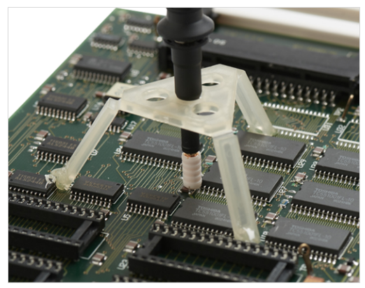
The size of the test point can also impact probe selection. Standard size probes and accessories are fine for probing connector pins, resistor leads, and back planes. However,for probing surface mount circuitry, smaller probes with accessories designed for surface mount applications are recommended.
Newer probes may be available with MMCX connectors. These connectors may be soldered onto circuit boards as either temporary or permanent test points. They can help maintain high signal fidelity by minimizing ground lead length and bringing shielding right to the device under test. Figure 4.3. shows how probes with MMCX connectors can be applied.
The goal is to select probe sizes, geometries, and accessories that best fit your particular application. This allows quick, easy, and solid connection of probes to test points for reliable measurements.
Understanding the Oscilloscope
Oscilloscope issues have as much bearing on probe selection as signal source issues. If the probe doesn’t match the oscilloscope, signal fidelity will be impaired at the oscilloscope end of the probe.
Bandwidth and Rise Time
It’s important to realize that the oscilloscope and its probes act together as a measurement system. Thus, the oscilloscope used should have bandwidth and rise time specifications that equal or exceed those of the probe used and that are adequate for the signals to be examined.
In general, the bandwidth and rise time interactions between probes and oscilloscopes are complex. Because of this complexity, most oscilloscope manufacturers specify oscilloscope bandwidth and rise time to the probe tip for specific probe models designed for use with specific oscilloscopes. To ensure adequate oscilloscope system bandwidth and rise time for the signals that you plan to examine, it’s best to follow the oscilloscope manufacturer’s probe recommendations.
Input Resistance and Capacitance
All oscilloscopes have input resistance and input capacitance. For maximum signal transfer the input R and C of the oscilloscope must match the R and C presented by the probe’s output as follows:
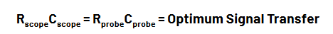
More specifically, 50 Ω oscilloscope inputs require 50 Ω probes, and 1 MΩ oscilloscope inputs require 1 MΩ probes. A 1 MΩ oscilloscope can also be used with a 50 Ω probe when the appropriate 50 Ω adapter is used.
Probe-to-oscilloscope capacitances must be matched as well. This is done through selection of probes designed for use with specific oscilloscope models. Additionally, many probes have a compensation adjustment to allow precise matching by compensating for minor capacitance variations. Whenever a probe is attached to an oscilloscope, the first thing that should be done is to adjust the probe’s compensation. Failing to properly match a probe to the oscilloscope – both through proper probe selection and proper compensation adjustment – can result in significant measurement errors.
Sensitivity
The oscilloscope’s vertical sensitivity range determines the overall dynamic range for signal amplitude measurement. For example, an oscilloscope with a 10-division vertical display range and a sensitivity range from 1 mV/division to 10 V/division has a practical vertical dynamic range from around 0.1 mV to 100 V. If the various signals that you intend to measure range in amplitude from 0.05 mV to 150 V, the base dynamic range of the example oscilloscope falls short at both the low and high ends. However, this shortcoming can be remedied by appropriate probe selection for the various signals that you’ll be dealing with.
For high-amplitude signals, the oscilloscope’s dynamic range can be extended upwards by using attenuator probes. For example, a 10X probe effectively shifts the oscilloscope’s sensitivity range upward by a decade, which would be 10 mV/division to 100 V/division for the example oscilloscope. Not only does this provide adequate range for your 150-volt signals, it gives you a top-end oscilloscope display range of 1000 volts. However, before connecting any probe to a signal make sure that the signal doesn’t exceed the probe’s maximum voltage capabilities.
Caution
Always observe the probe’s maximum specified voltage capabilities. Attaching the probe to a voltage in excess of those capabilities may result in personal injury as well as damage to equipment.
For low-amplitude signals, it’s possible to extend the range of the oscilloscope to lower sensitivities through use of a probe amplifier system. This typically is a differential amplifier, which could provide a sensitivity of 10 µV/division for example.
Such probe amplifier systems are highly specialized and are designed to match specific oscilloscope models. As a result, it’s important in making an oscilloscope selection to always check the manufacturer’s list of recommended accessories for available differential probe systems that meet your small-signal application requirements.
Caution
Differential probe systems often contain sensitive components that may be damaged by overvoltages, including static discharges. To avoid damage to the probe system, always follow the manufacturer’s recommendations and observe all precautions.
Readout Capability
Modern oscilloscopes provide on-screen readouts of their vertical and horizontal sensitivity settings (volts/division and seconds/division). Oftentimes, these oscilloscopes also provide probe sensing and readout processing so that the readout properly tracks the type of probe being used. For example, if a 10X probe is used, the oscilloscope should appropriately reflect that by adjusting the vertical readout by a 10X factor. Or if you’re using a current probe, the vertical readout is changed from volts/division to amps/ division to reflect the proper units of measurement.
The latest generation of probes support bidirectional communication between the probe and the oscilloscope. The TekVPI probe interface, for example, uses bidirectional communications. In addition to providing properly-scaled readout information on the oscilloscopes, it also enables the communication of error conditions from the probe to the oscilloscope. Scale factors and offsets can be controlled from the front panel of the oscilloscope. Procedures such as compensation and deskewing can also be done from the front panel.
To take advantage of such readout capability, it’s important to use probes that are compatible with the oscilloscope’s readout system. Again, this means following the manufacturer’s recommendations regarding probe usages with specific oscilloscopes. This is especially important for newer oscilloscopes which may have advanced readout features that may not be fully supported by many generic or commodity probes.
Selecting the Right Probe
From all of the preceding signal source and oscilloscope issues, it’s clear that selecting the right probe can be a daunting process without some assistance. In fact, since some key selection criteria – such as probe rise time and oscilloscope input capacitance – are not always specified, the selection process may be reduced to guesswork in some cases.
To avoid guesswork, it’s always best to select an oscilloscope that includes a wide selection of probes in the recommended accessories list. Also, when you encounter new measurement requirements, be sure to check with the manufacturer of your oscilloscope for newly introduced probes that may extend your oscilloscope’s capabilities.
And finally, keep in mind that there really is no “right” probe selection for any given application. There are only “right” oscilloscope/probe combination selections, and they rely on first defining your signal measurement requirements in terms of:
- Type of signal (voltage, current, optical, etc.)
- Signal frequency content (bandwidth issues)
- Signal rise time
- Source impedance (R and C)
- Signal amplitudes (maximum, minimum)
- Test point geometries (leaded component,surface mount, etc.)
By considering the above issues and filling in the blanks with information specific to your applications, you’ll be able to specify the oscilloscope and various compatible probes that will meet all of your application needs.
5. How Probes Affect Your Measurements
To obtain an oscilloscope display of a signal, some portion of the signal must be diverted to the oscilloscope’s input circuit. This is illustrated in Figure 5.1, where the circuitry behind the test point, TP, is represented by a signal source, Es, and the associated circuit impedances, Zs1 and Zs2, that are the normal load on Es. When an oscilloscope is attached to the test point, the probe impedance, Zp, and oscilloscope input impedance, Zi , become part of the load on the signal source.
Depending on the relative values of the impedances, addition of the probe and oscilloscope to the test point causes various loading effects.
This chapter explores loading effects, as well as other probing effects, in detail.
The Effect of Source Impedance
The value of the source impedance can significantly influence the net effect of any probe loading. For example, with low source impedances, the loading effect of a typical high-impedance 10X probe would be hardly noticeable. This is because a high impedance added in parallel with a low impedance produces no significant change in total impedance.
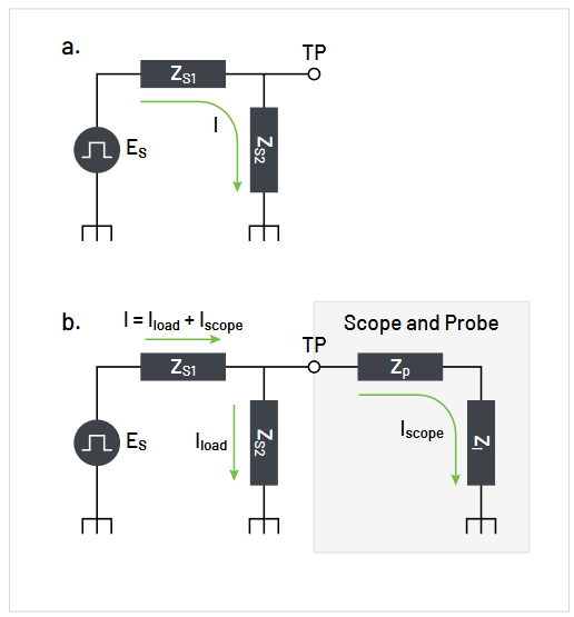
However, the story changes dramatically with higher source impedances. Consider, for example, the case where the source impedances in Figure 5.1 have the same value, and that value equals the total of the probe and oscilloscope impedances. This situation is illustrated in Figure 5.2.
For equal values of Z, the source load is 2Z without the probe and oscilloscope attached to the test point (see Figure 5.2a). This results in a signal amplitude of 0.5ES at the unprobed test point. However, when the probe and oscilloscope are attached (Figure 5.2b), the total load on the source becomes 1.5Z, and the signal amplitude at the test point is reduced to two-thirds of its unprobed value.
In this latter case, there are two approaches that can be taken to reduce the impedance loading effects of probing. One approach is to use a higher impedance probe. The other is to probe the signal somewhere else in the circuit at a test point that has a lower impedance. For example, cathodes, emitters, and sources usually have lower impedances than plates, collectors, or drains.
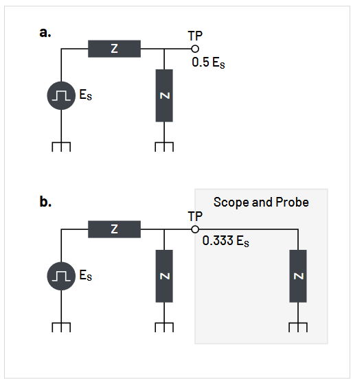
Capacitive Loading
As signal frequencies or transition speeds increase, the capacitive element of the impedances becomes predominant. Consequently, capacitive loading becomes a matter of increased concern. In particular, capacitive loading will affect the rise and fall times on fast-transition waveforms and the amplitudes of high-frequency components in waveforms.
Effect on Rise Time
To illustrate capacitive loading, let’s consider a pulse generator with a very fast rise time. This is shown in Figure 5.3, where the pulse at the ideal generator’s output has a rise time of zero (tr = 0). However, this zero rise time is modified through integration by the associated resistance and capacitance of the source impedance load.
The RC integration network always produces a 10% to 90% rise time of 2.2RC. This is derived from the universal timeconstant curve of a capacitor. The value of 2.2 is the number of RC time constants necessary for C to charge through R from the 10% value to the 90% amplitude value of the pulse.
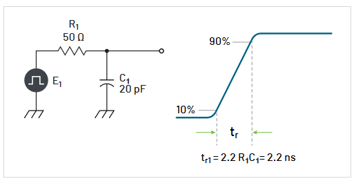
In the case of Figure 5.3, the 50 Ω and 20 pF of the source impedance results in a pulse rise time of 2.2 ns. This 2.2RC value is the fastest rise time that the pulse can have.
When the pulse generator’s output is probed, the probe’s input capacitance and resistance are added to that of the pulse generator. This is shown in Figure 5.4, where the 10 MΩ and 11 pF of a typical probe have been added. Since the probe’s 10 MΩ resistance is so much greater than the generator’s 50 Ω resistance, the probe’s resistance can be ignored. However, the probe’s capacitance is in parallel with the load capacitance and adds to it directly for a total load capacitance of 31 pF. This increases the value of 2.2RC and results in an increase in the measured rise time to 3.4 ns versus the 2.2 ns previous to probing.
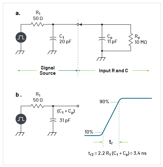
You can estimate the effect of probe tip capacitance on rise time by taking the ratio of the probe’s specified capacitance to the known or estimated source capacitance. Using the values from Figure 5.4 this would result in the following estimate of percentage change in rise time:
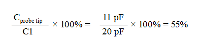
From the above, it’s clear that probe choice, especially with regard to probe capacitance, can affect your rise time measurements. For passive probes, the greater the attenuation ratio, the lower the tip capacitance in general. This is indicated in Table 4.1 which lists some probe capacitance examples for various passive probes.
Where smaller tip capacitance is needed, active FET-input probes should be used. Depending on the specific active probe model, tip capacitances of 1 pF and less are available.
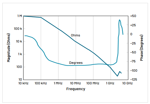
Effect on Amplitude and Phase
In addition to affecting rise time, capacitive loading also affects the amplitude and phase of the high-frequency components in a waveform. With regard to this, it is important to keep in mind that all waveforms are composed of sinusoidal components. A 50 MHz square wave will have harmonic components of significance beyond 100 MHz. Thus, it’s important to not only consider loading effects at a waveform’s fundamental frequency but also at frequencies several multiples above the fundamental.
Loading is determined by the total impedance at the probe tip. This is designated as Zp. Zp is composed of a resistive component, Rp, and reactive component Xp. The reactive component is predominantly capacitive, although inductive elements may be designed into the probe to partially offset capacitive loading.
As a rule, Zp decreases with increasing frequency. Most probe instruction manuals document probe Rp with curves showing Zp versus frequency. Figure 5.5 is an example of such a curve for a typical active probe. Notice that the 1 MΩ impedance magnitude is constant to nearly 100 kHz. This was done by careful design of the probe’s associated resistive, capacitive, and inductive elements.
Figure 5.6 shows another example of a probe curve. In this case Rp and Xp versus frequency are shown for a typical 10 MΩ passive probe. The dashed line (Xp) shows capacitive reactance versus frequency. Notice that Xp begins decreasing at DC, but Rp doesn’t start rolling off significantly until 100 kHz. (Theoretical resistance would not roll off, but real-world resistors such as Rp have parasitic capacitance in parallel with the resistance. This causes Rp to appear like a capacitor at very high frequencies.)
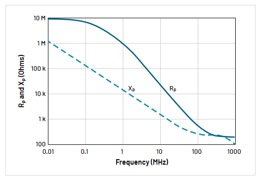
Again, the total loading has been offset by careful design of the associated R, C, and L elements.
If you don’t have access to a probe’s impedance curves, you can make a worst-case loading estimate using the following formula:
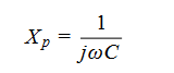
where:
Xp = capacitive reactance
ω = angular frequency
C = probe tip capacitance
For example, a standard passive 10 MΩ probe with a tip capacitance of 11 pF has a capacitive reactance (Xp) of about 290 Ω at 50 MHz. Depending on the signal source impedance, this loading could have a major effect on the signal amplitude (by simple divider action), and it could even affect the operation of the circuit being probed.
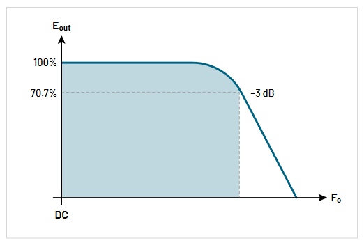
Bandwidth Considerations
Bandwidth is a measurement system issue that involves both the bandwidth of the probe and the oscilloscope. The oscilloscope’s bandwidth should exceed the predominant frequencies of the signals you want to measure, and the bandwidth of the probe used should equal or exceed the bandwidth of the oscilloscope.
From a measurement system perspective, the real concern is the bandwidth at the probe tip. Oftentimes manufacturers will specify bandwidth at the probe tip for certain oscilloscope/ probe combinations. This is not always the case, though. Consequently, you should be aware of the major bandwidth issues of an oscilloscope and a probe, both individually and in combination.
Oscilloscope Bandwidth
Bandwidth is defined as the point on an amplitude versus frequency plot where the measurement system is 3 dB down from the reference level. This is illustrated in Figure 5.7 which shows a response curve with the 3 dB point indicated. This curve is for an oscilloscope with a Guassian response, that is it rolls off at -20 dB/decade. This response is typical of general-purpose oscilloscopes with bandwidths below 1 GHz. The derating guidance in this primer applies to this class of oscilloscope. Higher-bandwidth oscilloscope often incorporate input filters with a much steeper rolloff, so derating is not as important on these instruments.
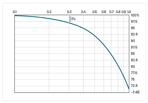
It’s important to note that the measurement system is 3 dB down in amplitude at its rated bandwidth. This means that you can expect 30% error in amplitude measurements for frequencies at the bandwidth limit.
Usually you won’t be using an oscilloscope at its full bandwidth limit. However, if amplitude accuracy is of paramount importance, you should be prepared to derate the oscilloscope’s bandwidth accordingly.
As an example, consider the expanded view of bandwidth roll-off shown in Figure 5.8. The horizontal scale in this figure shows the derating factor necessary to obtain amplitude accuracies better than 30%. With no derating (a factor of 1.0), a 100 MHz oscilloscope will have up to a 30% amplitude error at 100 MHz. If you want amplitude measurements to be within 3%, the bandwidth of this oscilloscope must be derated by a factor of 0.3 to 30 MHz. Anything beyond 30 MHz will have an amplitude error in excess of 3%.
The above example points out a general rule of thumb for oscilloscope selection. For amplitude measurements within 3%, select an oscilloscope with a specified bandwidth that’s three to five times greater than the highest frequency waveform that you’ll be measuring.
When rise time or fall time are the measurements of primary interest, you can convert a general-purpose oscilloscope’s bandwidth (BW) specification to a rise time specification with the following formula:
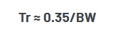
or, for convenience:
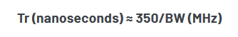
As with bandwidth, you should select an oscilloscope with a rise time that’s three to five time greater than the fastest rise time that you expect to measure. (Note that the constant 0.35 in the equation above assumes a Gaussian rolloff. Oscilloscopes with a bandwidth of <1 GHz typically have a 0.35 value, while oscilloscopes with a bandwidth of > 1 GHz usually have a value between 0.40 and 0.45.)
Probe Bandwidth
All probes, like other electronic circuits, have a bandwidth limit. And, like oscilloscopes, probes are typically ranked or specified by their bandwidth. Thus, a probe with a 100 MHz bandwidth will have an amplitude response that is 3 dB down at the 100 MHz point.
Similarly, probe bandwidth can also be expressed in terms of rise time by the same formula used for oscilloscopes (Tr ≈ 0.35/BW). Also, for active probes, the oscilloscope and probe rise times can be combined by the following formula to obtain an approximate probe/oscilloscope system rise time:
For passive probes, the relationship is more complex, and the above formula should not be used.
As a rule, probe bandwidth should always equal or exceed the bandwidth of the oscilloscope that it will be used with. Using a probe of lesser bandwidth will limit the oscilloscope to less than its full measurement capability. This is illustrated further in Figure 5.9, which shows the same pulse transition being measured with three probes of different bandwidths.
The first measurement, shown in Figure 5.9a, was made using a 10X, 1 GHz probe with 10 MΩ resistance and 3.9 pF capacitance. Note that the pulse rise time was measured as 2.162 ns. This is well within the 400 ps rise time range of the 10 GHz scope and 1 GHz probe combination.
Figure 5.9. Effects on rise time of three different probes: (a) 1 GHz, 10x probe, (b) 200 MHz, 10x probe, and (c) 20 MHz 1x probe. All measurements were made with the same 10 GHz oscilloscope.
Now look what happens when a 10X, 200 MHz probe is used to measure the same pulse with the same oscilloscope. This is shown in Figure 5.9b, where the measured rise time is now 3.002 ns. That’s nearly a 30% increase over the previous measurement of 2.162 ns!
As would be expected, the pulse’s observed rise time becomes even longer with a lower bandwidth probe. An extreme case is shown in Figure 5.9c, where a 1X, 20 MHz probe was used on the same pulse. Here the rise time has slowed from the original 2.162 ns to 30.30 ns.
The key takeaway here is that probe selection is imperative!
To get maximum performance from any oscilloscope – the performance that you paid for – be sure to use the manufacturer’s recommended probes.
Bandwidth to the Probe Tip
In general, the issues of probe bandwidth and resulting probe/oscilloscope system bandwidth should be resolved by following manufacturer’s specifications and recommendations. Tektronix, for example, specifies the bandwidth over which a probe will perform within specified limits. These limits include total aberrations, rise time, and swept bandwidth.
Also, when used with a compatible oscilloscope, a Tektronix probe extends the oscilloscope’s bandwidth to the probe tip. For example, a Tektronix 100 MHz probe provides 100 MHz performance (–3 dB) at the probe tip when used with a compatible 100 MHz oscilloscope.
The industry recognized test setup for verifying bandwidth to the probe tip is illustrated by the equivalent circuit in Figure 5.10. The test signal source is specified to be a 50 Ω source terminated in 50 Ω, resulting in an equivalent 25 Ω source termination. Additionally, the probe must be connected to the source by a probe-tip-to-BNC adaptor or its equivalent. This latter requirement for probe connection ensures the shortest possible ground path.
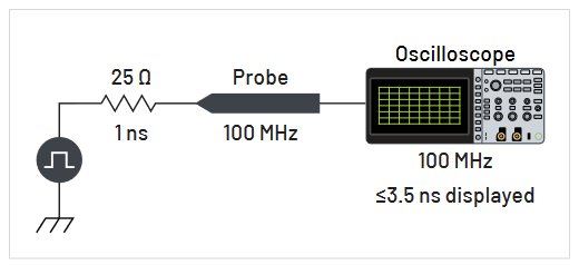
Using the above described test setup, a 100 MHz oscilloscope/probe combination should result in an observed rise time of < 3.5 ns. This 3.5 ns rise time corresponds to a 100 MHz bandwidth according to the previously discussed bandwidth/rise time relationship (Tr ≈ 0.35/BW).
Most manufacturers of general-purpose oscilloscopes that include standard accessory probes promise and deliver the advertised oscilloscope bandwidth at the probe tip.
However, it’s important to remember that bandwidth at the probe tip is determined by the test method of Figure 5.10. Since real-world signals rarely originate from 25 Ω sources, somewhat less than optimum response and bandwidth should be expected in real-world use — especially when measuring higher impedance circuits.
6. Probe Grounding and Ground Lead Effects
When making ground-referenced measurements, two connections to the circuit or device under test are necessary. One connection is made to the voltage signal or other parameter being measured. The other necessary connection is a ground return through the oscilloscope and back to the circuit under test. This ground return is necessary to complete the measurement current path.
In cases where the circuit under test and the grounded oscilloscope are plugged into the same power outlet circuit, the common of the power circuit provides a ground return path. In this case, one will see signals without connecting the ground lead. However, this signal return path through the power grounds is indirect and lengthy. Consequently it should not be relied on as a clean, low-inductance ground return. Instead, a ground connection should be made at the DUT and probes are designed to make this connection.
As a rule, when making any kind of oscilloscope measurement, you should use the shortest possible grounding path. This helps to minimize the effects of inductance on frequency response, we well as reducing the impact of noise. These effects are the main subject of this chapter.
Suspicion is the first defense against ground-lead problems. Always be suspicious of any noise or aberrations being observed on an oscilloscope display of a signal. The noise or aberrations may be part of the signal, or they may be the result of the measurement process. The following sections describes symptoms of grounding issues, guidelines for determining if aberrations are part of the measurement process and best practices on how to mitigate the impact on your measurements.
Ground Lead Length and Frequency Response
The length of ground leads has an impact on the frequency response of our probe, which can manifest as ringing and slowed rise times.
Ground paths, whether on a probe or in a circuit, have inductance and their impedance increases as signal frequency increases. Figure 6.1 shows the equivalent circuit of a probe connected to a device under test. Notice that there’s an inductance (L) associated with the ground lead. This ground-lead inductance increases with increasing lead length.
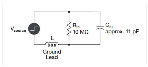
The ground lead reactive elements L and Cin form a series resonant circuit with only Rin for damping. When this series resonant circuit is hit with a pulse, it will ring. Not only will there be ringing, but excessive ground-lead inductance will limit the charging current to Cin and, thus, will limit the rise time of the pulse.
If the inductance is kept low enough, its impact on your measurements can be minimized. In order to see ringing or other aberrations caused by poor grounding, two conditions must exist:
- The oscilloscope system bandwidth must be high enough to “see” the high-frequency content of the signal at the probe tip.
- The input signal at the probe tip must contain enough high-frequency information (fast rise time) to cause the ringing or aberrations.
Without going into the mathematics, an 11 pF passive probe with 6-inch ground lead will ring at about 140 MHz when excited by a fast pulse. With a 100 MHz oscilloscope, this ringing is well above the bandwidth of the oscilloscope and may not be seen at all. But, with a faster oscilloscope, say 200 MHz, the ground lead induced ringing will be well within the oscilloscope’s bandwidth and will be apparent on the display of the pulse.
Figure 6.2 illustrates ground lead induced ringing. In Figure 6.2a, a matched oscilloscope/probe combination was used to acquire a fast transition. The ground lead used was the standard 6.5-inch probe ground clip, and it was attached to a common near the test point.
In Figure 6.2b, the same pulse transition is acquired. This time, however, the probe’s standard ground lead was extended with a 25-inch clip lead. This ground lead extension might be done, for example, to avoid having to move the ground clip each time different points are probed in a large system. Unfortunately, this practice increases the inductance in the ground path and can cause severe ringing, as shown.
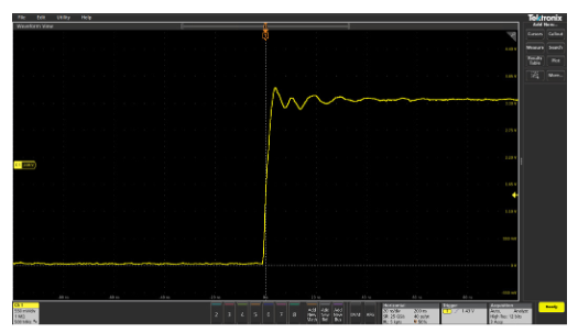
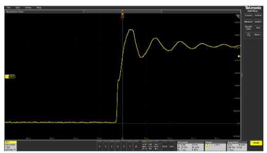
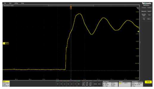
Figure 6.2. Ground lead length and placement can dramatically affect measurements.
Figure 6.2c shows the results of another variation of lengthening the ground loop. In this case, the probe’s ground lead wasn’t connected at all. Instead, a separate, 25-inch conductor was run from the circuit common to the oscilloscope chassis, effectively lengthening the ground path even more than the 25-inch probe clip lead used in Figure 6.2b. This resulted in the lower frequency ringing seen in Figure 6.2c.
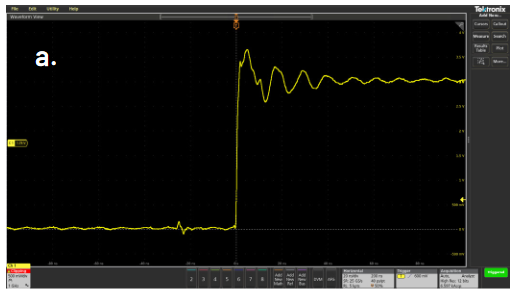
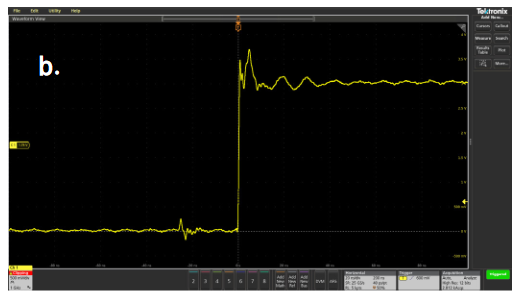
Figure 6.3. A fast step (1.5 ns Tr) has aberrations impressed on it due to use of a 12.5 inch probe ground lead (a). These aberrations can be changed by moving the probe cable or placing a hand over the cable (b).
From these examples, it’s clear that ground lead length can have a significant impact on measurement quality.
The position and environment of a long ground lead may also affect the capacitive characteristics of the signal path and therefore the quality of measurements. Figure 6.3 shows examples of ringing and aberrations on a 10 GHz oscilloscope using a probe a long 12.5 inch ground lead. This step signal has a very quick 1.5 ns rise time, so it has enough high frequency components to cause ringing within the probe’s ground circuit.
Both waveform displays in Figure 6.3 were obtained while acquiring the same step waveform with the same oscilloscope and probe. Notice, however, that the aberrations are slightly different between Figure 6.3a and 6.3b. The difference in Figure 6.3b was caused by repositioning the probe cable slightly and placing a hand over part of the probe cable. This caused a small change in the capacitance and high-frequency termination characteristics of the probe grounding circuitry, and thus, a change in the aberrations.
Determining the source of aberrations
The fact that the probe ground lead can cause aberrations on a waveform with fast transitions is an important point to realize. It’s also just as important to realize that aberrations seen on a waveform might just be part of the waveform, and not a result of the probe grounding method.
To distinguish between the two situations, move the probe cable around. If placing your hand over the probe or moving the cable causes a change in the aberrations, the aberrations are being caused by the probe grounding system. A correctly grounded (terminated) probe will be completely insensitive to cable positioning or touch.
If you see ringing on a pulse display, try shortening the length of your ground lead. A shorter ground lead has less inductance and will cause a higher frequency ringing. If you see the ringing frequency change on the pulse display, you’ll know that it’s ground-lead related. Shortening the ground lead further should move the ring frequency beyond the bandwidth of the oscilloscope, thereby minimizing its effect on your measurements. If the ringing doesn’t change when you change ground-lead length, then the ringing is probably coming from the circuit under test.
Noise Due to Poor Grounding Techniques
Noise is another type of signal distortion that can appear on oscilloscope waveform displays. As with ringing and aberrations, noise might actually be part of the signal at the probe tip, or it might appear on the signal as a result of poor grounding techniques. The difference is that the noise is generally from an external source, and its appearance is not a function of the speed of the signal being observed. In other words, poor grounding can result in noise appearing on any signal of any speed.
There are two primary mechanisms by which noise can be impressed on signals as a result of probing. One is by ground loop noise injection. The other is by inductive pickup through the probe cable or probe ground lead.
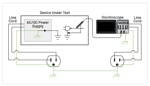
Ground Loop Noise Injection
Noise injection into the grounding system can be caused by unwanted current flow in the ground loop existing between the oscilloscope common, the test circuit power line grounds, and the probe ground lead and cable. Normally, all of these points are — or should be — at zero volts, and no ground current will flow. However, if the oscilloscope and test circuit are on different building system grounds, there could be small voltage differences or noise on one of the building ground systems. Figure 6.4 shows the ground connections in this scenario. Note that:
- A potential difference in any of the ground points in this system will cause current to flow in the ground loop.
- The current flow in the ground loop develops a voltage drop across the probe’s ground conductor.
- This noise voltage will be injected into the oscilloscope in series with the signal from the probe tip.
- The result is that you’ll see noise riding on the signal of interest
With ground loop noise injection, the noise is often line frequency noise (50 or 60 Hz). Just as often, though, the noise may be in the form of spikes or bursts resulting from building equipment — such as air conditioners — switching on and off.
Warning!
Never isolate the oscilloscope from ground by defeating the safety three-wire ground system on the power plug. This may result in metal surfaces becoming energized to hazardous voltage levels.
There are various things that can be done to avoid or minimize ground loop noise problems. The first approach is to minimize ground loops by using the same power circuits for the oscilloscope and circuit under test. Additionally, the probes and their cables should be kept away from sources of potential interference. In particular, don’t allow probe cables to lie alongside or across equipment power cables.
If ground loop noise problems persist, you can reduce the impact to your measurements by using a differential voltage probe, or better yet, an optically isolated probe to reject common mode noise.
Induced Noise
Noise can enter a common ground system by induction into probe cables, particularly when probes with long cables are used. Proximity to power lines or other current-carrying conductors can induce current flow in the probe’s outer cable shield. The circuit is completed through the building system common ground. To minimize this potential source of noise, use probes with shorter cables when possible, and always keep probe cables away from possible sources of interference.
Noise can enter a common ground system by induction into probe cables, particularly when probes with long cables are used. Proximity to power lines or other current-carrying conductors can induce current flow in the probe’s outer cable shield. The circuit is completed through the building system common ground. To minimize this potential source of noise, use probes with shorter cables when possible, and always keep probe cables away from possible sources of interference.
Noise can also be induced directly into the probe ground lead. This is the result of typical probe ground leads appearing as a single-turn loop antenna when connected to the test circuit. This ground lead antenna is particularly susceptible to electromagnetic interference from logic circuits or other fast changing signals. If the probe ground lead is positioned too close to certain areas on the circuit board under test — such as clock lines — the ground lead may pick up signals that will be mixed with the signal at the probe tip.
Determining the source of noise
When you see noise on an oscilloscope display of a signal, the question is: Does the noise really occur as part of the signal at the probe tip, or is it being induced into the probe ground lead? To answer this question, try moving the probe ground lead around. If the noise signal level changes, the noise is being induced into the ground lead.
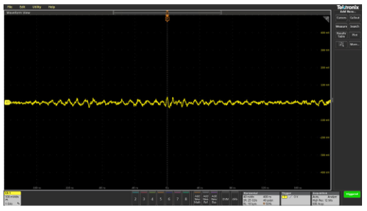
Another effective approach to noise source identification is to disconnect the probe from the circuit and clip the probe’s ground lead to the probe tip, then pass this probe-tip/ ground-lead loop antenna back and forth over the circuit. This loop antenna will pick up areas of strong radiated noise in the circuit. Figure 6.5 shows an example of what can be found on a logic circuit board by searching with the probe ground lead connected to the probe tip.
To minimize noise induced into the probe ground, keep ground leads away from noise sources on the board under test. Additionally, a shorter ground lead will reduce the amount of noise pick-up.
Grounding Best Practices
In general, the shortest ground path produces the best measurements. The ultimate grounding system is an incircuit PCB (printed circuit board) to probe-tip adapter, as shown in Figure 6.6. The PCB adaptor allows you to plug the probe tip directly into a circuit test point, and the outer barrel of the adaptor makes a direct and short ground contact to the ground ring at the probe’s tip.
For critical amplitude and timing measurements, it’s recommended that circuit board designs include PCB/ probe-tip adaptors for established test points. Not only does this clearly indicate test point locations, but it ensures the best possible connection to the test point for the most reliable oscilloscope measurements.
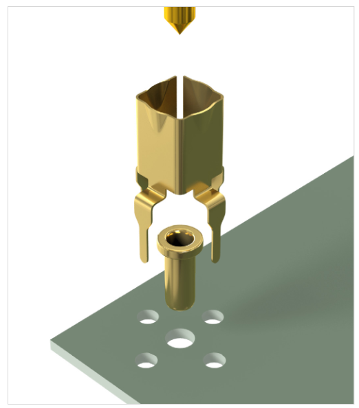
The waveform from Figure 6.3 was again acquired with the same oscilloscope and probe. Only this time, the six-inch probe ground lead was removed, and the step signal was acquired through a PCB to probe-tip adaptor installation. The resulting display of the aberration-free step waveform is shown in Figure 6.7. Elimination of the probe’s ground lead and direct termination of the probe in the PCB to probe-tip adaptor has eliminated virtually all the aberrations from the waveform display. The display is now an accurate portrayal of the step waveform at the test point.
Another option for providing a short ground path is to use an MMCX connector and compatible probe such as a TPP1000 1 GHz 10X passive probe. MMCX connectors are high-bandwidth coaxial connectors often used in RF applications. This makes them well-suited for use as test points, and they may be permanently installed or temporarily soldered in place. (Figure 4.3 shows an example of using MMCX connectors.)
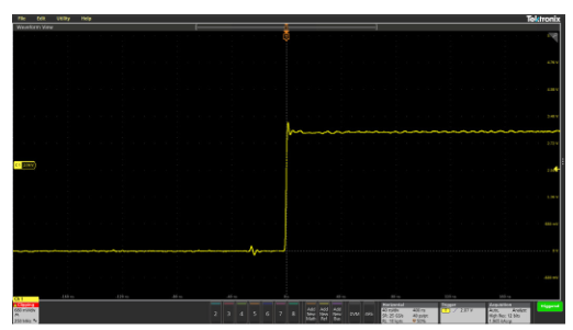
Unfortunately, permanently installed test points are not practical for many general-purpose measurement situations. Instead of using an adaptor, the most common approach is to use a short ground lead that’s clipped to a grounding point in the circuit under test. This is far more convenient because it allows you to quickly move the probe from point to point in the circuit under test. The short (usually 6-inch or 150 mm) ground lead that most probe manufacturers supply with their probes provides adequate results for many measurements, especially if you are measuring signals below 100 MHz or you can tolerate some normal ringing in your measurements.
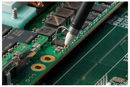
For high-frequency signals lower than 30 Vrms, a ground spring may be used to shorten the ground path. These springs attach to the grounded barrel of passive probes. They can be bent to adapt to connection points, and are convenient for probing across surface mount components such as the 0402 packaged capacitor shown in Figure 6.8.
Yet another alternative is to use an active FET probe. FET probes, because of their high input impedance and extremely low tip capacitance (often less than 1 pF), can reduce the ground lead problems often experienced with passive probes. This is illustrated in Figure 6.9.
Figure 6.9. Examples of ground lead effects for passive probes versus active probes. Effects on the waveform of 6.5 inch, 12.5 inch, and 25 inch ground leads used on a passive probe (a). Same waveform acquired using a 1.5 inch, 4.5 inch, and 10.5 inch ground lead with an active FET probe (b).
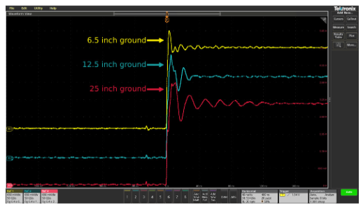
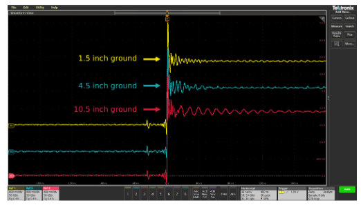
7. Differential Measurements
Strictly speaking, all voltage measurements are differential measurements. A standard oscilloscope measurement — where the probe is attached to a signal point, and the probe ground lead is attached to circuit ground — is actually a measurement of the signal difference between the test point and ground. In that sense, there are two signal lines – the ground signal line and the test signal line.
In practice, however, differential measurements refers to the measurement of two signal lines, both of which are above ground. This requires a method of finding the voltage difference between two signals and converting this difference into one signal line referenced to ground (single-ended signal) for input to the oscilloscope, as shown in Figure 7.7. The difference signal may be produced by a special amplifier that is part of the probing system, or if the oscilloscope allows waveform math, each signal line can be acquired on separate oscilloscope channels and the two channels algebraically subtracted. A probing system that includes a differential amplifier is called a differential voltage probe. In either case, rejection of the common-mode signal is a key concern in differential measurement quality
Understanding Difference and Common-mode Signals
An ideal differential amplifier amplifies the “difference”signal, VDM, between its two inputs and completely rejects any voltage which is common to both inputs, which is referred to as VCM. The result is an output voltage given by:
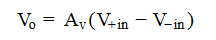
where:
Av = the amplifier’s gain
Vo = the output signal referenced to earth ground
The voltage of interest, or difference signal, is referred to as the differential voltage or differential mode signal and is expressed as VDM, where:
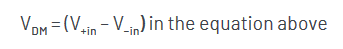
Notice that the common mode voltage, VCM, is not part of the above equation. That’s because the ideal differential amplifier rejects all of the common-mode component,regardless of its amplitude or frequency.
Figure 7.8 provides an example of using a differential amplifier to measure the gate drive of the upper MOSFET device in an inverter circuit. As the MOSFET switches on and off, the source voltage swings from the positive supply rail to the negative rail. A transformer allows the gate signal to be referenced to the source. The differential amplifier allows the oscilloscope to measure the true VGS signal (a few volt swing) at sufficient resolution, such as 2 V/division, while rejecting the several-hundred-volt transition of the source to ground.
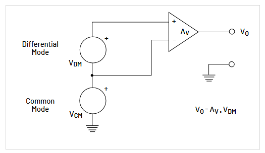
In real life, differential amplifiers cannot reject all of the common-mode signal. A small amount of common-mode voltage appears as an error signal in the output. This common-mode error signal is indistinguishable from the desired differential signal.
The ability of a differential amplifier to minimize undesirable common-mode signals is referred to as common-mode rejection ratio or CMRR for short. The true definition of CMRR is “differential-mode gain divided by common-mode gain referred to the input”:
For evaluation purposes, CMRR performance can be assessed with no input signal. The CMRR then becomes the apparent VDM seen at the output resulting from the commonmode input. This is expressed either as a ratio – such as 10,000:1 – or in dB:
For example, a CMRR of 10,000:1 is equivalent to 80 dB. To see the importance of this, suppose you need to measure the voltage in the output damping resistor of the audio power amplifier shown in Figure 7.9. At full load, the voltage across the damper (VDM) should reach 35 mV with an output swing (VCM) of 80 Vp-p. The differential amplifier being
used has a CMRR specification of 10,000:1 at 1 kHz. With the amplifier driven to full power with a 1 kHz sine wave, one ten thousandth of the common-mode signal will erroneously appear as VDM at the output of the differential amplifier, which would be 80 V/10,000 or 8 mV. The 8 mV of residual commonmode signal represents up to a 22% error in the true 35 mV signal!
It’s important to note that the CMRR specification is an absolute value. It doesn’t specify polarity or degrees of phase shift of the error. Therefore, you cannot simply subtract the error from the displayed waveform. Also, CMRR generally is highest (best) at DC and degrades with increasing frequency of VCM. Some differential amplifiers plot the CMRR specification as a function of frequency; others simply provide CMRR specifications at a few key frequencies. In either case, it’s important in comparing differential amplifiers or probes to be certain that your CMRR comparisons are at the same frequency or frequencies.
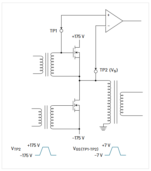
It’s also important to realize that CMRR specifications assume that the common-mode component is sinusoidal. This is often not the case in real-life. For example, the common-mode signal in the inverter of Figure 7.8 is a 30 kHz square wave. Since the square wave contains energy at frequencies considerably higher than 30 kHz, the CMRR will probably be worse than that specified at the 30 kHz point.
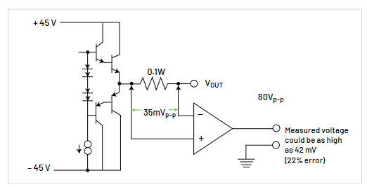
Whenever the common-mode component is not sinusoidal, an empirical test is the quickest way to determine the extent of the CMRR error (see Figure 7.10). Temporarily connect both input leads to the source. The oscilloscope is now displaying only the common-mode error. You can now determine if the magnitude of the error signal is significant. Remember, the phase difference between VCM and VDM is not specified. Therefore subtracting the displayed commonmode error from the differential measurement will not accurately cancel the error term.
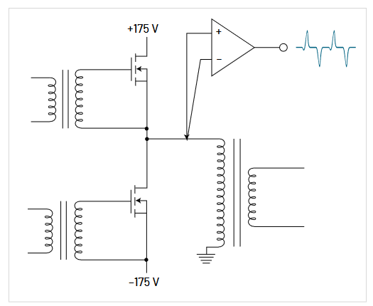
The test illustrated by Figure 7.10 is useful for determining the extent of common-mode rejection error in the actual measurement environment. However there’s one effect this test will not catch. With both inputs connected to the same point, there’s no difference in driving impedance as seen by the amplifier. This situation produces the best CMRR performance. But when the two inputs of a differential amplifier are driven from significantly different source impedances, the CMRR will be degraded.
Minimizing Differential Measurement Errors
Connecting the differential amplifier or probe to the signal source is generally the greatest source of error. To maintain the input match, both paths should be as identical as possible. Any cabling should be of the same length for both inputs.
If individual probes are used for each signal line, they should be the same model and cable length. When measuring lowfrequency signals with large common-mode voltages, avoid the use of attenuating probes. At high gains, they simply cannot be used as it’s impossible to precisely balance their attenuation.
Input cabling that’s spread apart acts as a transformer winding. Any AC magnetic field passing through the loop induces a voltage which appears to the amplifier input as differential and will be faithfully summed into the output! To minimize this, it’s common practice to twist the + and – input cables together in a pair. This reduces line frequency and other noise pick up. With the input leads twisted together, as indicated in Figure 7.11, any induced voltage tends to be in the VCM path, which is rejected by the differential amplifier.
High-frequency measurements subject to excessive common-mode can be improved by winding both input leads through a ferrite torroid. This attenuates high-frequency signals which are common to both inputs. Because the differential signals pass through the core in both directions, they’re unaffected.
The input connectors of most differential amplifiers are BNC connectors with the shell grounded. When using probes or coaxial input connections, there’s always a question of what to do with the grounds. Because measurement applications vary, there are no precise rules.
When measuring low-level signals at low frequencies, it’s generally best to connect the grounds only at the amplifier end and leave both unconnected at the input end.
This provides a return path for any currents induced into the shield, but doesn’t create a ground loop which may upset the measurement or the device-under-test.
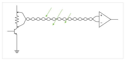
At higher frequencies, the probe input capacitance, along with the lead inductance, forms a series resonant “tank” circuit, which may ring. In single-ended measurements, this effect can be minimized by using the shortest possible ground lead. This lowers the inductance, effectively moving the resonating frequency higher, hopefully beyond the bandwidth of the amplifier. Differential measurements are made between two probe tips, and the concept of ground does not enter into the measurement. However, if the ring is generated from a fast rise of the commonmode component, using a short ground lead reduces the inductance in the resonant circuit, thus reducing the ring component. In some situations, a ring resulting from fast differential signals may also be reduced by attaching the ground lead. This is the case if the common-mode source has very low impedance to ground at high frequencies, i.e. is bypassed with capacitors. If this isn’t the case, attaching the ground lead may make the situation worse! If this happens, try grounding the probes together at the input ends. This lowers the effective inductance through the shield.
Of course, connecting the probe ground to the circuit may generate a ground loop. This usually doesn’t cause a problem when measuring higher-frequency signals. The best advice when measuring high frequencies is to try making the measurement with and without the ground lead; then use the setup which gives the best results.
When connecting the probe ground lead to the circuit, remember to connect it to ground! It’s easy to forget where the ground connection is when using differential amplifiers since they can probe anywhere in the circuit without the risk of damage.
8. Measuring Low-amplitude Signals
Measuring low-amplitude signals presents a unique set of challenges. Foremost of these challenges are the problems of noise and adequate measurement sensitivity.
Noise Reduction
Ambient noise levels that would be considered negligible when measuring signals of a few hundred millivolts or more are no longer negligible when measuring signals of tens of millivolts or less. Consequently, minimizing ground loops and keeping ground leads short are imperatives for reducing noise pick up by the measurement system. At the extreme, power-line filters and a shielded room may be necessary for noise-free measurement of very low amplitude signals.
However, before resorting to extremes, you should consider signal averaging as a simple and inexpensive solution to noise problems. If the signal you’re trying to measure is repetitive and the noise that you’re trying to eliminate is random, signal averaging can provide extraordinary improvements in the SNR (signal-to-noise ratio) of the acquired signal. An example of this is shown in Figure 8.1.
Signal averaging is a standard function of most digital oscilloscopes. It operates by summing multiple acquisitions of the repetitive waveform and computing an average waveform from the multiple acquisitions. Since random noise has a long-term average value of zero, the process of signal averaging reduces random noise on the repetitive signal. The amount of improvement is expressed in terms of SNR. Ideally, signal averaging improves SNR by 3 dB per power of two averages. Thus, averaging just two waveform acquisitions (21 ) provides up to 3 dB of SNR improvement, averaging four acquisitions (22) provides 6 dB of improvement, eight averages (23) provides 9 dB of improvement, and so on.
Increasing Measurement Sensitivity
An oscilloscope’s measurement sensitivity is a function of its input circuitry. The input circuitry either amplifies or attenuates the input signal for an amplitude calibrated display of the signal on the oscilloscope screen. The amount of amplification or attenuation needed for displaying a signal is selected via the oscilloscope’s vertical sensitivity setting, which is adjusted in terms of volts per display division (V/div).
Figure 8.1. A noisy signal (a) can be cleaned up by a signal averaging (b).
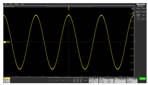
In order to display and measure small signals, the oscilloscope input must have enough gain or sensitivity to provide at least a few divisions of signal display height. For example, to provide a two-division high display of a 20 mV p-to-p signal, the oscilloscope would require a vertical sensitivity setting of 10 mV/div. For the same two-division display of a 10 mV signal, the higher sensitivity setting of 5 mV/div would be needed. Note that a low volts-per-division setting corresponds to high sensitivity and vice versa.
In addition to the requirement of adequate oscilloscope sensitivity for measuring small signals, you’ll also need an adequate probe. Typically, this will not be the usual probe supplied as a standard accessory with most oscilloscopes. Standard accessory probes are usually 10X probes, which reduce oscilloscope sensitivity by a factor of 10. In other words, a 5 mV/div oscilloscope setting becomes a 50 mV/div setting when a 10X probe is used. Consequently, to maintain the highest signal measurement sensitivity of the oscilloscope, you’ll need to use a non-attenuating 1X probe.
However, as discussed in previous chapters, remember that 1X passive probes have lower bandwidths, lower input impedance, and generally higher tip capacitance. This means that you’ll need to be extra cautious about the bandwidth limit of the small signals you’re measuring and the possibility of signal source loading by the probe. If any of these appear to be a problem, then a better approach is to take advantage of the much higher bandwidths and lower loading typical of 1X active probes.
In cases where the small signal amplitude is below the oscilloscope’s sensitivity range, some form of preamplification will be necessary. Because of the noise susceptibility of the very small signals, differential preamplification is generally used. The differential preamplification offers the advantage of some noise immunity through common-mode rejection, and the advantage of amplifying the small signal so that it will be within the sensitivity range of the oscilloscope.
With differential preamplifiers designed for oscilloscope use, sensitivities on the order of 10 µV/div can be attained.
These specially designed preamplifiers have features that allow useable oscilloscope measurements on signals as small as 5 µV, even in high noise environments!
Remember, though, taking full advantage of a differential preamplifier requires use of a matched set of high-quality passive probes. Failing to use matched probes will defeat the common-mode noise rejection capabilities of the differential preamplifier.
Also, in cases where you need to make single-ended rather than differential measurements, the negative signal probe can be attached to the test circuit ground. This, in essence, is a differential measurement between the signal line and signal ground. However, in doing this, you lose commonmode noise rejection since there will not be noise common to both the signal line and ground.
As a final note, always follow the manufacturer’s recommended procedures for attaching and using all probes and probe amplifiers. Also, with active probes in particular, be extra cautious about over-voltages that may damage voltage-sensitive probe components.
9. What To Do About Probing Effects
From the preceding examples and discussions, we’ve seen that the signal source impedance, the probe, and the oscilloscope form an interactive system. For optimum measurement results, you need to do everything possible to minimize the oscilloscope/probe affects on the signal source.
The following general rules apply:
- Always match your oscilloscope and probes according to the oscilloscope manufacturer’s recommendations.
- Make sure that your oscilloscope/probe has adequate bandwidth or rise time capabilities for the signal you’re trying to measure. Ideally, you should select a oscilloscope/probe combination with a rise time specification that’s three to five times faster than the fastest rise time you plan to measure.
- Always keep your probe ground leads as short and direct as possible. Excessive ground loops can cause ringing on pulses.
- Select the probes that best match your application’s needs in terms of both measurement capabilities and mechanical attachment to test points.
- Finally, always be aware of the possible probe loading effects on the circuit being probed. Remember that probe capacitance has a bigger impact as signal frequency increases. In many cases, loading can be controlled or minimized through probe selection.
The following summarizes some of the probe loading considerations to be aware of for different types of probes.
Passive Probes
1X passive probes typically have a lower resistance and higher capacitance than 10X passive probes. As a result, 1X probes are more prone to cause loading, and whenever possible 10X probes should be used for general-purpose probing.
Voltage Divider (Zo) Probes
These probes have very low tip capacitance, but at the expense of relatively high resistive loading. They’re intended for use where impedance matching is required in 50 Ω environments. However, because of their very high bandwidth/rise time capabilities, voltage divider probes are often used in other environments for high-speed timing measurements. For amplitude measurements, the effect of the probe’s low input R should be taken into account.
Active Probes
Active probes can provide the best of both worlds with very low resistive loading and very low tip capacitance. The trade-off is that active probes typically have a low dynamic range. However, if your measurements fit within the range of an active probe, this can be the best choice in many cases.
10. Understanding Probe Specifications
Most of the key probe specifications have been discussed in preceding chapters, either in terms of probe types or in terms of how probes affect measurements.
This chapter gathers all of those key probe specification parameters and terms into one place for easier reference.
The following list of specifications is presented in alphabetical order; not all of these specifications will apply to any given probe. For example, insertion impedance is a specification that applies to current probes only. Other specifications, such as bandwidth, are universal and apply to all probes.
Aberrations (universal)
An aberration is any amplitude deviation from the expected or ideal response to an input signal. In practice, aberrations usually occur immediately after fast waveform transitions and appear as what’s sometimes referred to as “ringing.”
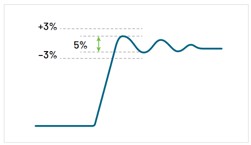
Aberrations are measured, or specified, as a ± percentage deviation from the final pulse response level (see Figure 10.1). This specification might also include a time window for the aberrations. An example of this would be:
Aberrations should not exceed ±3% or 5% peak-to-peak within the first 30 nanoseconds.
When excessive aberrations are seen on a pulse measurement, be sure to consider all possible sources before assuming that the aberrations are the fault of the probe. For example, are the aberrations actually part of the signal source? Or are they the result of the probe grounding technique?
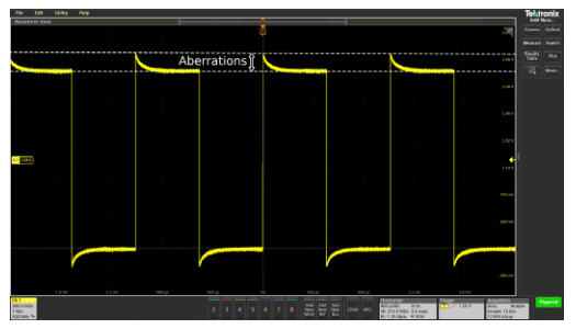
One of the most common sources of observed aberrations is neglecting to check and properly adjust the compensation of voltage probes. A severely over-compensated probe will result in significant peaks immediately following pulse edges (see Figure 10.2).
Accuracy (universal)
For voltage-sensing probes, accuracy generally refers to the probe’s attenuation of a DC signal. The calculations and measurements of probe accuracy generally should include the oscilloscope’s input resistance. Thus, a probe’s accuracy specification is only correct or applicable when the probe is being used with an oscilloscope having the assumed input resistance. An example attenuation accuracy specification would be:
10X within 3% (for oscilloscope input of 1 MΩ ±2%)
For current-sensing probes, the accuracy specification refers to the accuracy of the current-to-voltage conversion. This depends on the current transformer turns ratio and the value and accuracy of the terminating resistance. Current probes that work with dedicated amplifiers have outputs that are calibrated directly in amps/div and have accuracy specifications that are given in terms of attenuator accuracy as a percentage of the current/division setting.
Amp-Second Product (current probes)
For current probes, amp-second product specifies the energy handling capability of the current transformer’s core. If the product of the average current and pulse width exceeds the amp-second rating, the core saturates. This core saturation results in a clipping off or suppression of those portions of the waveform occurring during saturation. If the amp-second product is not exceeded, the signal voltage output of the probe will be linear and the measurement accurate.
Attenuation Factor (universal)
All probes have an attenuation factor, and some probes may have selectable attenuation factors. Typical attenuation factors are 1X, 10X, and 100X.
The attenuation factor is the amount by which the probe reduces signal amplitude. A 1X probe doesn’t reduce — or attenuate — the signal, while a 10X probe reduces the signal to 1/10th of its probe tip amplitude. Probe attenuation factors allow the measurement range of an oscilloscope to be extended. For example, a 100X probe allows signals of 100 times greater amplitude to be measured.
The 1X, 10X, 100X designations stem from the days when oscilloscopes didn’t automatically sense probe attenuation and adjust scale factor accordingly. The 10X designation, for example, reminded you that all amplitude measurements needed to be multiplied by 10. The readout systems on many modern oscilloscopes automatically sense probe attenuation factors and adjust the scale factor readouts accordingly.
Voltage probe attenuation factors are achieved using resistive voltage divider techniques. Consequently, probes with higher attenuation factors typically have higher input resistances. Also the divider effect splits probe capacitance, effectively presenting lower probe tip capacitance for higher attenuation factors.
Bandwidth (universal)
All probes have bandwidth. A 10 MHz probe has a 10 MHz bandwidth, and a 100 MHz probe has a 100 MHz bandwidth. The bandwidth of a probe is that frequency where the probe’s response causes output amplitude to fall to 70.7% (–3 dB), as indicated in Figure 10.3.
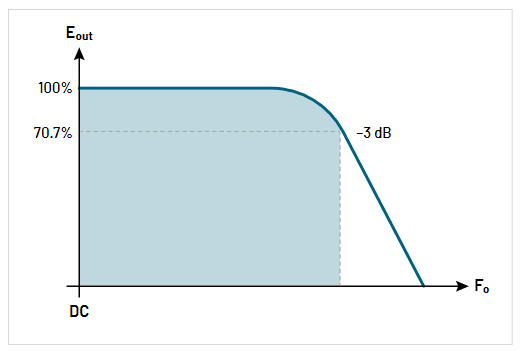
It should also be noted that some probes have a lowfrequency bandwidth limit as well. This is the case, for example, with AC current probes. Because of their design, AC current probes cannot pass DC or low-frequency signals. Thus, their bandwidth must be specified with two values, one for low frequency and one for high frequency.
For oscilloscope measurements, the real concern is the overall bandwidth of the oscilloscope and probe combined. This system performance is what ultimately determines measurement capability. Unfortunately, attaching a probe to an oscilloscope results in some degradation of bandwidth performance. For example, using a 100 MHz generic probe with a 100 MHz oscilloscope results in a measurement system with a bandwidth performance that is something less than 100 MHz. To avoid the uncertainty of overall system bandwidth performance, Tektronix specifies its passive voltage probes to provide a specified measurement system bandwidth at the probe tip when used with the designated oscilloscope models.
In selecting oscilloscopes and oscilloscope probes, it’s important to realize that bandwidth has several implications for measurement accuracy.
In terms of amplitude measurements, a sine wave’s amplitude becomes increasingly attenuated as the sine wave frequency approaches the bandwidth limit. At the bandwidth limit, the sine wave’s amplitude will be measured as being 70.7% of its actual amplitude. Thus, for greater amplitude measurement accuracy, it’s necessary to select oscilloscopes and probes with bandwidths several times greater than the highest frequency waveform that you plan to measure.
The same holds true for measuring waveform rise and fall times. Waveform transitions, such as pulse and square wave edges, are made up of high-frequency components. Attenuation of these high-frequency components by a bandwidth limit results in the transition appearing slower than it really is. For accurate rise and fall time measurements, it’s necessary to use a measurement system with adequate bandwidth to preserve the high frequencies that make up the waveform’s rise and fall times. This is most often stated in terms of a measurement system rise time, which should typically be four to five times faster than the rise times that you are trying to measure.
Capacitance (universal)
Generally, probe capacitance specifications refer to the capacitance at the probe tip. This is the capacitance that the probe adds to the circuit test point or device under test.
Probe tip capacitance (Figure 10.4) is important because it affects how pulses are measured. A low tip capacitance minimizes errors in making rise time measurements. Also, if a pulse’s duration is less than five times the probe’s RC time constant, the amplitude of the pulse is affected because the signal falls before reaching its maximum amplitude.
Probes also present a capacitance to the input of the oscilloscope, and this probe capacitance should match that of the oscilloscope. For 10X and 100X probes, this capacitance is referred to as a compensation range, which is different than tip capacitance. For probe matching, the oscilloscope’s input capacitance should be within the compensation range of the probe.
CMRR (differential probes)
Common-mode rejection ratio (CMRR) is a differential probe’s ability to reject any signal that is common to both test points in a differential measurement. CMRR is a key figure of merit for differential probes and amplifiers, and it is defined by:
where:
Ad= the voltage gain for the difference signal
Ac= the voltage gain for common-mode signal
Ideally, Ad should be large, while Ac should equalize to zero, resulting in an infinite CMRR. In practice, a CMRR of 10,000:1 is considered quite good. What this means is that a common-mode input signal of 5 volts will be rejected to the point where it appears as 0.5 millivolts at the output. Such rejection is important for measuring difference signals in the presence of noise.
Since CMRR decreases with increasing frequency, the frequency at which CMRR is specified is as important as the CMRR value. A differential probe with a high CMRR at a high frequency is better than a differential probe with the same CMRR at a lower frequency
Optically isolated probes are a special category of probes with extremely high CMRR which they achieve by galvanic isolation between the probe head and oscilloscope.
Decay Time Constant (current probes)
The decay time constant specification indicates a current probe’s pulse supporting capability. This time constant is the secondary inductance (probe coil) divided by the terminating resistance. The decay time constant is sometimes called the probe L/R ratio.
With larger L/R ratios, longer current pulses can be represented without significant decay or droop in amplitude. With smaller L/R ratios, long- duration pulses will be seen as decaying to zero before the pulse is actually completed.
Direct Current (current probes)
Direct current (DC) decreases the permeability of a current probe’s coil core. This decreased permeability results in a decreased coil inductance and L/R time constant. The result is reduced coupling performance for low frequencies and loss of measurement response for low-frequency currents. Some AC current probes offer current-bucking options that null the effects of DC.
Frequency Derating (current probes)
Current probe specifications should include amplitude versus frequency derating curves that relate core saturation to increasing frequency. The effect of core saturation with increasing frequency is that a waveform with an average current of zero amps will experience clipping of amplitude peaks as the waveform’s frequency or amplitude is increased.
with an average current of zero amps will experience clipping of amplitude peaks as the waveform’s frequency or amplitude is increased.
nsertion Impedance (current probes)
Insertion impedance is the impedance that is transformed from the current probe’s coil (the secondary) into the current carrying conductor (the primary) that’s being measured. Typically, a current probe’s reflected impedance values are in the range of milliOhms and present an insignificant effect on circuits of 25Ω or more impedance.
Input Capacitance (universal)
The probe capacitance measured at the probe tip.
Input Resistance (universal)
A probe’s input resistance is the impedance that the probe places on the test point at zero Hertz (DC).
Maximum Input Current Rating (current probes)
The maximum input current rating is the total current (DC plus peak AC) that the probe will accept and still perform as specified. In AC current measurements, peak-to-peak values must be derated versus frequency to calculate the maximum total input current.
Maximum Peak Pulse Current Rating(current probes)
This rating should not be exceeded. It takes into account core saturation and development of potentially damaging secondary voltages. The maximum peak pulse current rating is usually stated as an amp-second product.
Maximum Voltage Rating (universal)
Voltages approaching a probe’s maximum rating should be avoided. The maximum voltage rating is determined by the breakdown voltage rating of the probe body or the probe components at the measuring point.
Propagation Delay (universal)
Every probe offers some small amount of time delay or phase shift that varies with signal frequency. This is a function of the probe components and the time it takes for the signal to travel through these components from probe tip to oscilloscope connector.
Usually, the most significant shift is caused by the probe cable. For example, a 42-inch section of special probe cable has a 5 ns signal delay. For a 1 MHz signal, the 5 ns delay results in a two-degree phase shift. A longer cable results in correspondingly longer signal delays.
Propagation delay is usually only a concern when comparative measurements are being made between two or more waveforms. For example, when measuring time differences between two waveforms, the waveforms should be acquired using matched probes so that each signal experiences the same propagation delay through the probes.
Another example would be making power measurements by using a voltage probe and a current probe in combination. Since voltage and current probes are of markedly different construction, they will have different propagation delays. Whether or not these delays will have an effect on the power measurement depends on the frequencies of the waveforms being measured. For Hz and kHz signals, the delay differences will generally be insignificant. However, for MHz signals the delay differences may have a noticeable effect.
Rise Time (universal)
A probe’s 10% to 90% response to a step function indicates the fastest transition that the probe can transmit from tip to oscilloscope input. For accurate rise and fall time measurements on pulses, the measurement system’s rise time (oscilloscope and probe combined) should be three to five times faster than the fastest transition to be measured.
Tangential Noise (active probes)
Tangential noise is a method of specifying probe-generated noise in active probes. Tangential noise Figure are approximately two times the RMS noise.
Temperature Range (universal)
Current probes have a maximum operating temperature that’s the result of heating effects from energy induced into the coil’s magnetic shielding. Increasing temperature corresponds to increased losses. Because of this, current probes have a maximum amplitude versus frequency derating curve.
Attenuator voltage probes (i.e., 10X, 100X, etc.) may be subject to accuracy changes due to changes in temperature.
Threshold Voltage (logic)
A logic probe measures and analyzes signals differently than other oscilloscope probes. The logic probe doesn’t measure analog details. Instead, it detects logic threshold levels. When you connect a mixed signal oscilloscope to a digital circuit using a logic probe, you’re only concerned with the logic state of the signal. At this point there are just two logic levels of concern. When the input is above the threshold voltage (Vth) the level is said to be “high” or “1”. Conversely, the level below Vth is a “low” or “0”. When input is sampled, the mixed signal oscilloscope stores a “1” or a “0” depending on the level of the signal relative to the voltage threshold.
The large number of signals that can be captured at one time by the logic probe is what sets it apart from the other oscilloscope probes. These digital acquisition probes connect to the device under test and the probe’s internal comparator is where the input voltage is compared against the threshold voltage (Vth), and where the decision about the signal’s logic state (1 or 0) is made. The threshold value is set by the user, ranging from TTL levels to CMOS, ECL, and user-definable.