
Introduction
Embedded systems are literally everywhere in our society today. A simple definition of an embedded system is a specialpurpose computer system that is part of a larger system or machine with the intended purpose of providing monitoring and control services to that system or machine. The typical embedded system starts running some special purpose application as soon as it is turned on and will not stop until it is turned off. Virtually every electronic device designed and produced today is an embedded system. A short list of embedded system examples include:
- Automatic teller machines
- Cellular phones
- Computer printers
- Antilock brake controllers
- Microwave ovens
- Inertial guidance systems for missiles
- DVD players
- Programmable logic controllers (PLC) for industrial
- automation and monitoring
- Portable music players
- Maybe even your toaster…

Embedded systems can contain many different types of devices including microprocessors, microcontrollers, DSPs, RAM, EPROMs, FPGAs, A/Ds, D/As, and I/O. These various devices have traditionally communicated with each other and the outside world using wide parallel buses. Today, however, more and more of the building blocks used in embedded system design are replacing these wide parallel buses with serial buses for the following reasons:
- Less board space required due to fewer signals to route
- Lower cost
- Lower power requirements
- Fewer pins on packages
- Embedded clocks
- Differential signaling for better noise immunity
- Wide availability of components using standard serial interfaces
While serial buses provide a number of advantages, they also pose some significant challenges to an embedded system designer due simply to the fact that information is being transmitted in a serial fashion rather than parallel. This application note discusses common challenges for embedded system designers and how to overcome them using capabilities found in the following series of oscilloscopes: the 5 Series MSO, and the MSO/DPO70000, DPO7000, MSO/DPO5000, MDO4000, MDO3000, and MSO/DPO2000 Series.

Parallel vs. Serial
With a parallel architecture, each component of the bus has its own signal path. There may be 16 address lines,16 data lines, a clock line and various other control signals. Address or data values sent over the bus are transferred at the same time over all the parallel lines. This makes it relatively easy to trigger on the event of interest using either the State or Pattern triggering found in most oscilloscopes and logic analyzers. It also makes it easy to understand at a glance the data you capture on either the oscilloscope or logic analyzer display. For example, in Figure 1 we’ve used a logic analyzer to acquire the clock, address, data and control lines from a microcontroller. By using a state trigger, we’ve isolated the bus transfer we’re looking for. To “decode” what’s happening on the bus, all we have to do is look at the logical state of each of the address, data, and control lines. With a serial bus all this information is sent serially on a few conductors (sometimes one). This means that a single signal may include address, control, data, and clock information. As an example, look at the Controller Area Network (CAN) serial signal shown in Figure 2.
This message contains a start of frame, an identifier (address), a data length code, data, CRC, and end of frame as well as a few other control bits. To further complicate matters, the clock is embedded in the data and bit stuffing is used to ensure an adequate number of edges for the receiving device to lock to the clock. Even to the very trained eye, it would be extremely difficult to quickly interpret the content of this message. Now imagine this is a faulty message that only occurs once a day and you need to trigger on it. Traditional oscilloscopes and logic analyzers are simply not well equipped to deal with this type of signal.

Even with a simpler serial standard such as I2C, it is still significantly harder to observe what is being transmitted over the bus than it is with a parallel protocol.
I2C uses separate clock and data lines, so at least in this case you can use the clock as a reference point. However, you still need to find the start of the message (data going low while the clock is high), manually inspect and write down the data value on every rising edge of the clock, and then organize the bits into the message structure.
It can easily take a couple of minutes of work just to decode a single message in a long acquisition and you have no idea if that’s the message you are actually looking for. If it’s not, then you need to start this tedious and error prone process over on the next one. It would be nice to just trigger on the message content you are looking for, however the state and pattern triggers you’ve used for years on scopes and logic analyzers won’t do you any good here. They are designed to look at a pattern occurring at the same time across multiple channels. To work on a serial bus, their trigger engines would need to be tens to hundreds of states deep (one state per bit). Even if this trigger capability existed, it would not be a fun task programming it state-by-state for all these bits. There has to be a better way!
There is a better way. The following sections highlight how Tektronix oscilloscopes1 can be used with some of the most common low-speed serial standards used in embedded system design.
1 Support for serial bus standards vary depending on the oscilloscope model. For a table of buses supported by different Tektronix oscilloscopes, please see Appendix A or visit www.tektronix.com.

I2C
Background
I2C, or “I squared C”, stands for Inter-Integrated Circuit. It was originally developed by Philips in the early 1980s to provide a low-cost way of connecting controllers to peripheral chips in TV sets, but has since evolved into a worldwide standard for communication between devices in embedded systems. The simple two-wire design has found its way into a wide variety of chips like I/O, A/Ds, D/As, temperature sensors, microcontrollers and microprocessors from numerous leading chipmakers including: Analog Devices, Atmel, Infineon, Cyprus, Intel, Maxim, Philips, Silicon Laboratories, ST Microelectronics, Texas Instruments, Xicor, and others.
How It Works
I2C’s physical two-wire interface is comprised of bi-directional serial clock (SCL) and data (SDA) lines. I2 C supports multiple masters and slaves on the bus, but only one master may be active at a time. Any I2 C device can be attached to the bus allowing any master device to exchange information with a slave device. Each device is recognized by a unique address. A device can operate as either a transmitter or a receiver, depending on its function. Initially, I2 C only used 7-bit addresses, but evolved to allow 10-bit addressing as well. Three bit rates are supported: 100 kb/s (standard modep>,400 kb/s (fast mode), and 3.4 Mb/s (high-speed mode). The maximum number of devices is determined by a maximum capacitance of 400 pF or roughly 20-30 devices.
The I2C standard specifies the following format in Figure 4:
-
Start - indicates the device is taking control of the bus and that a message will follow.
- Address - a 7 or 10 bit number representing the address of the device that will either be read from or written to.
- R/W Bit - one bit indicating if the data will be read from or written to the device.
- Ack - one bit from the slave device acknowledging the master’s actions. Usually each address and data byte has an acknowledge, but not always.
- Data - an integer number of bytes read from or written to the device.
- Stop - indicates the message is complete and the master has released the bus.
There are two ways to group I2 C addresses for decoding: in 7-bits plus a read or write (R/W) bit scheme, and in 8-bits (a byte) where the R/W bit is included as part of the address. The 7-bit address scheme is the specified I2 C Standard followed by firmware and software design engineers. But many other engineers use the 8-bit address scheme. Tektronix oscilloscopes can decode data in either scheme.
Working with I2C
With the optional serial triggering and analysis capability, Tektronix oscilloscopes become powerful tools for embedded system designers working with I2 C buses. The front panel has Bus buttons that allow the user to define inputs to the scope as a bus. The I2 C bus setup menu is shown in Figure 5.
By simply defining which channels clock and data are on, along with the thresholds used to determine logic ones and zeroes, you’ve enabled the oscilloscope to understand the protocol being transmitted across the bus. With this knowledge, the oscilloscope can trigger on any specified message-level information and then decode the resulting acquisition into meaningful, easily interpreted results. Gone are the days of edge triggering, hoping you acquired the event of interest, and then manually decoding message after message while looking for the problem.
As an example, consider the embedded system in Figure 6. An I2 C bus is connected to multiple devices including a CPU, an EEPROM, a fan speed controller, a digital to analog converter (DAC), and a couple of temperature sensors.
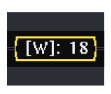
This instrument was returned to engineering for failure analysis as the product was consistently getting too hot and shutting itself off. The first thing to check is the fan controller and the fans themselves, but they both appear to be working correctly. The next thing to check for is a faulty temperature sensor. The fan speed controller polls the two temperature sensors (located in different areas of the instrument) periodically and adjusts the fan speed to regulate internal temperature. We are suspicious that one or both of these temperature sensors is not reading correctly. To see the interaction between the sensors and the fan speed controller, we simply need to connect to the I2 C clock and data lines and set up a bus. We know that the two sensors are addresses 18 and 19 on


the I2 C bus, so we decide to set up a trigger event to look for a write to address 18 (the fan speed controller polling the sensor for the current temperature). The triggered acquisition is shown in the screenshot Figure 7.
| Bus Condition | Indicated by: |
| Starts are indicated by vertical green bars. Repeated starts occur when another start is shown without a previous Stop. |
 |
| Addresses are shown in yellow boxes along with a [W] for write or [R] for read. Address values can be displayed in either hex or binary. |
 |
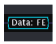
| Data is shown in cyan boxes. Data values can be displayed in either hex or binary. |
 |
| Missing Acks are indicated by an exclamation point inside a red box. |
 |
| Stops are indicated by red vertical bars |
 |
Table 1. Bus conditions
In this case, channel 1 (yellow) is connected to SCLK and channel 2 (cyan) to SDA. The purple waveform is the I2 C bus we’ve defined by inputting just a few simple parameters to the oscilloscope. The upper portion of the display shows the entire acquisition. In this case we’ve captured a lot of bus idle time with a burst of activity in the middle which we’ve zoomed in on. The lower, larger portion of the display is the zoom window. As you can see, the oscilloscope has decoded the content of each message going across the bus. Buses use the colors and marks in Table 1 to indicate important parts of the message. Taking a look at the acquired waveforms, we can see that the oscilloscope did indeed trigger on a Write to address 18 (shown in the lower left of the display). In fact, the fan speed controller attempted to write to address 18 twice, but in both cases it did not receive an acknowledge after
attempting to write to the temperature sensor. It then checked the temperature sensor at Address 19 and received back the desired information. So, why isn’t the first temperature sensor responding to the fan controller? Taking a look at the part on the board we find that one of the address lines isn’t soldered correctly. The temperature sensor was not able to communicate on the bus and the unit was overheating as a result. We’ve managed to isolate this potentially elusive problem in a matter of a couple minutes due to the I2 C trigger and bus decoding capability of the oscilloscope.
In the example in Figure 7 we triggered on a write, but the oscilloscope's powerful I2 C triggering includes many other capabilities:
- Start - triggers when SDA goes low while SCL is high.
- Repeated Start - triggers when a start condition occurs without a previous stop condition. This is usually when a master sends multiple messages without releasing the bus.
- Stop - triggers when SDA goes high while SCL is high.
- Missing Ack - slaves are often configured to transmit an acknowledge after each byte of address and data. The oscilloscope can trigger on cases where the slave does not generate the acknowledge bit.
- Address - triggers on a user specified address or any of the pre-programmed special addresses including General Call,Start Byte, HS-mode, EEPROM, or CBUS. Addressing can be either 7 or 10 bits and is entered in binary or hex.
- Data - triggers on up to 12 bytes of user specified data values entered in either binary or hex.
- Address and Data - this allows you to enter both address and data values as well as read vs. write to capture the exact event of interest.
These triggers allow you to isolate the particular bus traffic you’re interested in, while the decoding capability enables you to instantly see the content of every message transmitted over the bus in your acquisition.

SPI
Background
The Serial Peripheral Interface bus (SPI) was originally developed by Motorola in the late 1980s for their 68000 series micro-controllers. Due to the simplicity and popularity of the bus, many other manufacturers have adopted the standard over the years. It is now found in a broad array of components commonly used in embedded system design. SPI is primarily used between micro-controllers and their immediate peripheral devices. It’s commonly found in cell phones, PDAs, and other mobile devices to communicate data between the CPU, keyboard, display, and memory chips.
How It Works
The SPI bus is a master/slave, 4-wire serial communications bus. The four signals are clock (SCLK), master output/ slave input (MOSI), master input/slave output (MISO), and slave select (SS). Whenever two devices communicate, one is referred to as the "master" and the other as the “slave”. The master drives the serial clock. Data is simultaneously transmitted and received, making it a full-duplex protocol. Rather than having unique addresses for each device on the bus, SPI uses the SS line to specify which device data is being transferred to or from. As such, each unique device on the bus needs its own SS signal from the master. If there are 3 slave devices, there are 3 SS leads from the master, one to each slave as shown in Figure 8.

In Figure 8, each slave only talks to the master. However,SPI can be wired with the slave devices daisy-chained, each performing an operation in turn, and then sending the results back to the master as shown in Figure 9.
So, as you can see, there is no “standard” for SPI implementation. In some cases, where communication from the slave back to the master is not required, the MISO signal may be left out altogether. In other cases there is only one master and one slave device and the SS signal is tied to ground. This is commonly referred to as 2-wire SPI.
When an SPI data transfer occurs, an 8-bit data word is shifted out on MOSI while a different 8-bit data word is being shifted in on MISO. This can be viewed as a 16-bit circular shift register. When a transfer occurs, this 16-bit shift register is shifted 8 positions, thus exchanging the 8-bit data between the master and slave devices. A pair of registers, clock polarity (CPOL) and clock phase (CPHA) determine the edges of the clock on which the data is driven. Each register has two possible states which allows for four possible combinations, all of which are incompatible with one another. So a master/slave pair must use the same parameter values to communicate. If multiple slaves are used that are fixed in different configurations, the master will have to reconfigure itself each time it needs to communicate with a different slave.
Working with SPI
Using the front panel Bus buttons we can define an SPI bus by simply entering the basic parameters of the bus including which channels SCLK, SS, MOSI, and MISO are on,thresholds, and polarities (see Figure 10).
As an example, consider the embedded system in Figure 11.
An SPI bus is connected to a synthesizer, a DAC, and some I/O. The synthesizer is connected to a VCO that provides a 2.5 GHz clock to the rest of the system. The synthesizer is supposed to be programmed by the CPU at startup. However, something isn’t working correctly as the VCO is stuck at its rail generating 3 GHz. The first step in debugging this problem is to inspect the signals between the CPU and the synthesizer to be sure the signals are present and there are no physical connection problems, but we don’t find anything wrong. Next we decide to take a look at the information being transmitted across the SPI bus to program the synthesizer. To capture the information we set the oscilloscope to trigger on the synthesizer’s Slave Select signal going active and power up the DUT to capture the start-up programming commands. The acquisition is shown in Figure 12.
Channel 1 (yellow) is SCLK, channel 2 (cyan) is MOSI and channel 3 (magenta) is SS. To help determine if we’re programming the device correctly we take a look at the data sheet for the synthesizer. The first three messages on the bus are supposed to initialize the synthesizer, load the divider ratio, and latch the data. According to the spec, the last nibble (single hex character) in the first three transfers should be 3, 0, and 1, respectively, but we’re seeing 0, 0, and 0.


Upon seeing all 0s at the end of the messages we realize we’ve made one of the most common mistakes with SPI by programming the bits in each 24-bit word in reverse order in the software. A quick change in the software results in the following acquisition and a VCO correctly locked at 2.5 GHz as shown in Figure 13.
In the example above we used a simple SS Active trigger. The full SPI triggering capability in Tektronix oscilloscopes include the following types:
- SS Active - triggers when the slave select line goes true for a slave device.
- Start of Frame - triggers at the start of a frame when the clock idle time is used to define the frame timing.
- MOSI - trigger on up to 16 bytes of user specified data from the master to a slave.
- MISO - trigger on up to 16 bytes of user specified data from a slave to the master.
- MOSI/MISO - trigger on up to 16 bytes of user specified data for both master to slave and slave to master (available only on 4000/3000/2000 Series models.
Again, these triggers allow you to isolate the particular bus traffic you’re interested in, while the decoding capability enables you to instantly see the content of every message transmitted over the bus in your acquisition.
| USB Speed | Bit Rate | Bit Period |
| Low-Speed USB 2.0 | 1.5 Mbps | 667 ns |
| Full-Speed USB 2.0 | 12 Mbps | 83.3 ns |
| High-Speed USB 2.0 | 480 Mbps | 2.08 ns |
| SuperSpeed USB 3.0 | 5 Gbps | 200 ps |
Table 2. USB speeds.
USB
Background
The Universal Serial Bus (USB) has become a dominant interface on today’s personal computers, replacing many of the external serial and parallel buses previously used. Since its introduction in 1995, USB has grown beyond its original personal computer usage and has become a ubiquitous interface used in many types of electronic devices.
The USB 2.0 specification released in 2000 covers most of the USB devices that are being used today. USB 2.0 replaced the USB 1.1 specification, adding a high-speed interface (see Table 2) to the low-speed and full-speed interfaces in the USB 1.1 specification.
USB has expanded beyond just system-to-system communication. For example, the Inter-Chip USB (IC_USB) and the High-Speed Inter-Chip (HSIC) USB are used for chip-to-chip communications. Supplements to the USB 2.0 specification cover IC_USB, HSIC and other enhancements.
In 2008, the USB 3.0 specification was released. USB 3.0 is called SuperSpeed USB and is ten times faster than high-speed USB 2.0. SuperSpeed USB preserves backward compatibility with USB 2.0 devices. USB 3.0 is an additional specification that is used in conjunction with the USB 2.0 specification and does not replace it. SuperSpeed USB devices must implement USB 2.0 device framework commands and descriptors.

The USB Implementers Forum (USB-IF) manages and promotes USB standards and USB technology. USB specifications are available at the USB-IF web site at www.usb.org.
How It Works
The USB configuration is one host controller with 1 to 127 devices. USB is a tiered-star topology with optional hubs to expand the bus (Figure 14). The host is the only master and it controls all bus traffic. The host initiates all device communications and devices do not have the capability to interrupt the host.
There are four USB speeds as shown in Table 2. A high-speed device starts out at full-speed and then transitions to highspeed. The speed of a USB 2.0 bus is limited by the slowest device connected to the host controller.
With SuperSpeed USB, two host controllers are used: one for SuperSpeed USB devices and one for USB 2.0 devices. Like a USB 2.0 system, the speed of the bus with USB 2.0 devices is limited by the slowest device.

Device Endpoints
Device endpoints are data sources and sinks in the device. Each device can have up to 16 data endpoints (Figure 15). Endpoint 0 is mandatory and is used by the host to communicate to the device. A pipe is the logical connection between the application software in the host and device endpoint.
Enumeration
Enumeration is the configuration process that occurs at power-on or when a device is hot plugged. The host detects the presence of the device on the USB bus. Next, the host polls the device with the SETUP token using address 0 and endpoint 0. Then, the host assigns a unique address to the device in the range of 1 to 127. Also, the host identifies the device speed and data transfer type. During enumeration a device’s class is determined. The device class defines a device’s functionality such as printer, mass storage, video, audio, human interface, etc.

Electrical Configuration
The host uses an upstream “A” connector and devices use a downstream “B” connector, as shown in Figure 16. Each connector has three versions: standard, mini and micro.
The USB 2.0 cable has four wires as shown in Figure 16. Two wires are used to provide power from the host: 5 V power (red wire) and ground (black wire). The connectors are designed so that the power and ground pins are connected before the data pins. The host provides current from 100 mA to 500 mA with intelligent power management. For example, power to a device can be monitored by the host or hub and switched off if an over-current condition occurs.
| USB Speed | Low State | High State |
| Low-Speed | <0.3V | >2.8V |
| Full-Speed | <0.3V | >2.8V |
| High-Speed | 0 V±10% | 400 mV±10% |
Table 3. Electrical signal characteristics.
| USB Packet Type | Packet | Binary Value |
| Token | OUT IN SOF SETUP |
0001 1001 0101 1101 |
| Data | DATA0 DATA1 DATA2 MDATA |
0011 1011 0111 1111 |
| Handshake | ACK NAK STALL NYET |
0010 1010 1110 0110 |
| Special | PRE ERR SPLIT PING Reserved |
1100 1100 1000 0100 0000 |
Table 4. USB packet types.
A twisted differential pair Data+ (D+ green wire) and Data- (D- white wire) wires are used for bidirectional communications using half-duplex differential signaling controlled by the host.Signal levels are listed in Table 3. The bus is DC coupled.
The host pulls down both D+ and D- when no device is connected. This is called single-ended zero (SE0) state. The USB bus voltage is pulled positive or negative when a device is connected to the USB bus and the polarity indicates the speed of the device.

In the J idle state, a low-speed device pulls D- high resulting in a negative differential voltage. A full-speed device pulls D+ high resulting in a positive differential voltage. The K state is opposite of the J state.
Data transmission uses non return to zero inverted (NRZI)encoding with bit stuffing to ensure a minimum number of transitions. The least significant bit is transmitted first and the most significant bit is transmitted last.
Packets
The packets are the fundamental elements of USB communications. Packets start with a synchronization field followed by the packet identifier. After the packet identifier is no field or other fields depending upon the type of packet. The end-of-packet field terminates the packet.
Starting from the J idle state, a packet starts with an 8-bit synchronization (SYNC) field for low-speed and full-speed USB. SYNC is 3 KJ pairs followed by two Ks (Figure 17).
The SYNC field for high-speed USB is 15 KJ pairs followed by two Ks and hubs are allowed to reduce the repeating SYNC field to 5 KJ pairs followed by two Ks.
Packet identifier (PID) is the second packet byte composed of a 4-bit PID and its 4-bit PID complement for error checking. A PID encoding error is when the first PID 4-bits do not match the complement of the last PID 4-bits. Bits are sent out onto the bus least-significant bit first and most-significant bit last.
The PID 4-bit value identifies 17 types of packets as shown in Table 4. Notice packet PRE and ERR have the same PID code. Packet type groups are token, data, handshake and special.
The end-of-packet (EOP) is three bits long. EOP starts with two bits of SE0 and ends with one bit of J state.


Handshake Packets
Handshake packets such as data packet accepted (ACK) and data packet not accepted (NAK) are composed of the Sync byte, PID byte and EOP as seen in Figure 18.
Token Packets
Host sent token packets are composed of the SYNC, PID followed by two bytes composed of an 11-bit address and 5-bit cyclic redundancy check (CRC) (Figure 19).
The OUT, IN and SETUP tokens 11-bit address is subdivided into a 7-bit device address and a 4-bit endpoint identifier.Address zero is special and is for a device that has not been assigned an address at the beginning of the enumeration process. Later in the enumeration process the host assigns a nonzero address to the device.
All devices have an endpoint zero. Endpoint zero is used for device control and status. Other device endpoints are for data sources and/or sinks.
The host sends an OUT token to a device followed by a data packet. The host sends an IN token to a device and expects to receive a data packet or handshake packet such as NAK from the device.
Data Packets
Data packets contain a PID byte, data bytes and 16-bit CRC as shown in Figure 20.
DATA0 and DATA1 packets have a 1-bit sequence number that is used in stop and wait automatic repeat-request handshake. DATA0 and DATA1 packets alternate in error free transmission. Data packets are resent with the same sequence number when a transmission error occurs.
An error free data transaction is when the host sends a DATA0 packet to the device, the device sends a handshake ACK packet and then the host sends a DATA1 packet.
If the host does not receive a handshake ACK packet or received a NAK from the device, it resends the DATA0 packet.If the device sent an ACK packet and receives the data packet with the same sequence number, the device acknowledges the data packet but ignores the data as a duplicate.
Start of Frame
Start of Frame (SOF) packet, shown in Figure 21, is used to synchronize isochronous and polled data flows. The 11-bit frame number is incremented by one in each consecutive SOF.

Working with USB 2.0
USB serial triggering and analysis support is available on select Tektronix oscilloscopes (see Appendix A). For lowspeed and full-speed USB, trigger, decode and search support is provided by all of the oscilloscope models. For high-speed USB, a ≥1 GHz oscilloscope model is required.
As an example, the data latency performance of a full-speed memory device is checked by seeing if the memory device responds with NAK to the computer IN token request for data from the memory device.
A TDP1000 Differential Probe is used to probe a USB extension cable between the computer and the USB memory device. Before connecting the probe to the cable, we use the TDP1000 menu button on the probe to AutoZero the probe’s 4.25 V range.
To define a USB bus, we go to the bus menu and select USB from the list of supported standards. We then follow the setup buttons from left to right to define the parameters of our bus:speed, source channels, type of probe, and thresholds. The full-speed preset 1.4 V and -1.4 V thresholds are used in this example.
First, we can check the enumeration process by triggering on the SETUP token. After enumeration, we can verify the Start of Frame (SOF) packets by triggering on them and verifying the speed by checking if the J idle state is positive or by measuring the bit width of the SOF SYNC field.
Next, we can configure the oscilloscope to trigger on a NAK token and then put the oscilloscope in Single acquisition mode. We then have the computer request data from the memory device. If the memory device is ready to transfer data, the oscilloscope will not trigger. But, if the memory device is not ready to transfer data, it will send a NAK in response to the computer host IN token and the oscilloscope will trigger on the NAK. Figure 22 shows the NAK acquisition.

We can also copy the oscilloscope trigger settings to be the search criteria for Wave Inspector. Wave Inspector will search through the entire acquisition looking for every instance of a NAK. In this case, Wave Inspector found 11 NAKs. The first NAK is at the trigger position and the other 10 NAKs are after the trigger. All NAKs are in response to the computer host resending the IN token. Each NAK is easily viewed by using Wave Inspector next and previous front-panel buttons to jump to each marked NAK.
Available USB triggering capability includes the following types:
- SYNC
- Reset
- Suspend
- Resume
- End of Packet (EOP)
- Token (Address) Packet – SETUP, IN, OUT and SOF
- Data Packet – Any data value, DATA0, DATA1, DATA2 or MDATA – Data matching with up to 16 data bytes of pattern
- Handshake packets – Any handshake value, or ACK, NAK, STALL, or NYET
- Special packets – Reserved, PRE, or ERR, SPLIT, or PING
- Error types include PID Check Bits, Token CRC5, Data CRC16 or Bit stuffing
Wave Inspector can also search on all of the same criteria used for triggering.
With Tektronix oscilloscopes, you can easily capture and analyze USB 2.0 signals, protocol, and data and then correlate them to other analog and digital signals to provide you with complete design visibility.

Ethernet
Background
Ethernet is a family of frame-based computer networking technologies for local area networks (LANs), initially developed at Xerox PARC in the early 1970s. The first standard draft was published in 1980 by the Institute of Electrical and Electronics Engineers (IEEE). Approval of IEEE 802.3 CSMA/CD occurred in 1982 and the international ISO/IEEE 802.3 standard was approved in 1984.
How It Works
Two of the most common versions of Ethernet are 10BASE-T and 100BASE-TX which are found on most personal computers. The leading number represents the data rate in Mb/s. BASE indicates that the signals are baseband signals and there is no RF signal modulation. The T denotes the twisted pair wires that are in the LAN cable that is used between network nodes.
The popularity of 10BASE-T and 100BASE-TX and its decreasing hardware implementation cost has caused it to be incorporated in an increasing number of embedded systems designs.
Ethernet provides peer-to-peer packet-based communication, enabling direct point-to-point communication. At the physical layer, the 10BASE-T and 100BASE-TX signals transport address, control, data, and clock information. The data is transferred in sequences of data bytes called packets. Ethernet packets can carry other, higher-level protocol packets inside of them. For example, an Ethernet packet may contain an Internet Protocol (IP) packet, which in turn may contain a Transmission Control Protocol (TCP) packet. This signal complexity makes isolating events of interest difficult when analyzing 10BASE-T and 100BASE-TX waveforms.
The Ethernet data frame format is defined by the IEEE 802.3 standard and contains seven fields, as shown in Figure 24.
The Preamble is seven bytes long consisting of an alternating pattern of ones and zeros for synchronization.
The Start-of-frame Delimiter is a single byte with alternating ones and zeros but ending in two ones.
The Destination and Source Media Access Control (MAC) Addresses are each six bytes long, transmitted in mostsignificant to least-significant bit order. Each Ethernet node is assigned a unique MAC address which is used to specify both the destination and the source of each data packet. It thus forms the basis of most of the Link layer (OSI Layer 2) networking upon which upper layer protocols rely to produce complex, functioning networks.
The Length/Type field is a two-byte value. If the decimal value of Length/Type is ≤1500, it represents the number of data bytes in the data field. If the value of Length/Type is >1536 (0x0600), it is an EtherType value which specifies the protocol that is encapsulated in the payload of the Ethernet frame. (For example, EtherType is set to 0x0800 for IPv4.)
The Data packet contains 46 to 1500 bytes. If the data is less than 46 bytes long, the data field is padded to be 46 bytes long.
The Frame Check Sequence is a 32-bit cyclic redundancy check (CRC) and provides error checking across the Destination Address, Source Address, Length/Type and Data fields.
Finally, after each frame has been sent, transmitters are required to transmit a minimum of 12 bytes of idle characters before transmitting the next frame, or they must remain idle for an equal amount of time by de-asserting the transmit enable signal.

Working With Ethernet
Ethernet is becoming widely used in embedded designs today. Analyzing Ethernet traffic, both at the physical and protocol layers, can provide insight into the operation of other subsystems in the embedded design. However, a single differential Ethernet signal includes address, control, data, and clock information, which can make isolating events of interest difficult. Ethernet Serial Triggering and Analysis options transform select Tektronix oscilloscopes into robust tools for debugging 10BASE-T and 100BASE-TX-based systems with automatic trigger, decode, and search.
The oscilloscope can trigger on Ethernet packet content such as Start Frame Delimiter, MAC addresses, MAC length/type,MAC client data, Q-tag control information, IP header, TCP header, TCP/IPv4 client data, End of Packet, Idle (100BASETX and DPO4ENET only), and FCS (CRC) errors.
The decoded display provides a higher-level, combined view of the individual signals that make up 10BASE-T and 100BASE-TX, making it easy to identify where packets begin and end and identifying sub-packet components such as preamble, SFD, MAC addresses, Data, FSC, errors, etc. Each packet on the bus is decoded, and the value can be displayed in hex, binary, or ASCII in the bus waveform.
In addition to seeing decoded packet data on the bus waveform itself, you can view all captured packets in a tabular view much like you would see in a software listing. Packets are time stamped and listed consecutively with columns for each component (Time, Destination Address, Source Address,Length, Data, FCS/CRC, Errors).
Serial triggering is very useful for isolating the event of interest, but once you’ve captured it and need to analyze the surrounding data, what do you do? Simply use Wave Inspector to automatically search through the acquired data for user-defined criteria including serial packet content. Each occurrence is highlighted by a search mark. Rapid navigation between marks is as simple as pressing thePrevious(←) and Next (→) buttons on the oscilloscope front panel.
RS-232
Background
RS-232 is a widely-used standard for serial communication between two devices over a short distance. It is best known for its use in older PC serial ports, but it is also used in embedded systems as a debug port or for linking two devices.
The RS-232-C standard was introduced in 1969. The standard has been revised twice since then, but the changes are minor and the signals are interoperable with RS-232-C.There are also related standards, such as RS-422 and RS-485, which are similar but use differential signaling to communicate over longer distances.
How it Works
The two devices are referred to as the DTE (data terminal equipment) and DCE (data circuit-terminating equipment). In some applications, the DTE device controls the DCE device;in other applications, the two devices are peers and the distinction between DTE and DCE is arbitrary.
The RS-232 standard specifies numerous signals, many of which are not commonly used. The two most important signals are Transmitted Data (Tx) and Received Data (Rx). Tx carries data from the DTE to the DCE. The DTE device’s Tx line is the DCE device’s Rx line. Similarly, Rx carries data from the DCE to the DTE.
The RS-232 standard does not specify which connectors to use. Twenty-five-pin and nine-pin connectors are most common. Other connectors have ten, eight, or six pins. It’s also possible to connect two RS-232 devices on the same board, without using standard connectors.
| Signal | Abbreviation | Pin |
| Carrier Detect | DCD | 1 |
| Received Data | Rx | 2 |
| Transmitted Data | Tx | 3 |
| Data Terminal Ready | DTR | 4 |
| Common Ground | G | 5 |
| Data Set Ready | DSR | 6 |
| Request to Send | RTS | 7 |
| Clear to Send | CTS | 8 |
| Ring Indicator | RI | 9 |
Table 5. Common RS-232 connector pinout.
When connecting two RS-232 devices, a null modem is commonly required. This device swaps several lines, including the Tx and Rx lines. That way, each device can send data on its Tx line and receive data on its Rx line.
Table 5 shows the pinout used for a 9-pin connector,commonly used with RS-232 signals. Remember that if your signal has passed through a null modem, many of the signals will be swapped. Most importantly, Tx and Rx will be swapped.

When probing RS-232 signals, it is often helpful to use a breakout box. This device allows you to easily probe the signals inside an RS-232 cable. Breakout boxes are inexpensive and readily available from electronics dealers.
The RS-232 standard does not specify the content transmitted across the bus. ASCII text is most common, but binary data is also used. The data is often broken up into packets. With ASCII text, packets are commonly terminated by a new line or carriage return character. With binary data other values, such as 00 or FF hex are commonly used.
Devices often implement RS-232 using a universal asynchronous receiver/transmitter (UART). UARTs are widely available in off-the-shelf parts. The UART uses a shift register to convert a byte of data into a serial stream, and vice versa.In embedded designs, UARTs can also communicate directly without the use of RS-232 transceivers.
Figure 26 shows one byte of RS-232 data. The byte is composed of these bits.
- Start - The byte begins with a start bit.
- Data - Several bits of data follow.
Eight bits of data is the most common; some applications use seven bits of data. Even when only seven bits are transmitted, the data is often informally referred to as a byte. In UART to UART communication, 9 bit data words are sometimes used. - Parity - An optional parity bit.
- Stop - 1, 1.5, or 2 stop bits.
Working With RS-232
Serial triggering and analysis for the RS-232 bus is available on most Tektronix oscilloscopes (see Appendix A). You can view your RS-232, RS-422, RS-485, or UART data conveniently on your oscilloscope, without needing to attach to a PC or a specialized decoder.
Using the front-panel bus buttons we can define an RS-232 bus by entering basic parameters, such as the channels being used, bit rate, and parity (see Figure 27).
In this example, we have chosen ASCII decoding; the oscilloscope can also display RS-232 data as binary or hex.
Imagine you have a device that polls a sensor for data over an RS-232 bus. The sensor isn’t responding to requests for data.You want to find out if the sensor isn’t receiving the requests,or if it is receiving the requests but ignoring them.
First, probe the Tx and Rx lines and set up a bus on the oscilloscope. Then set the oscilloscope to trigger when the request for data is sent across the Tx line. The triggered acquisition is shown in Figure 28.
Here, we can see the Tx line on digital channel 1, and the Rx line on digital channel 0. But we’re more interested in the decoded data, shown above the raw waveforms. We’ve zoomed in to look at the response from the sensor. The overview shows the request on the Tx line and the response on the Rx line. The cursors show us that the reply comes around 37 ms after the end of the request. Increasing the controller’s timeout fixes the problem by giving enough time for the sensor to reply.


The oscilloscope’s RS-232 trigger includes these capabilities:
- Tx Start Bit - triggers on the bit indicating the start of a byte.
- Tx End of Packet - triggers on the last byte in a packet. A packet can be ended by a specific byte: Null (00 hex),linefeed (0A hex), carriage return (0D hex), space (20 hex),or FF hex.
- Tx Data - triggers on up to 10 bytes of user-specified data values.
- Rx Start Bit, Rx End of Packet, and Rx Data - these are like the Tx triggers, but on the Rx line.
With Tektronix oscilloscopes, you can easily view RS-232 signals, analyze them, and correlate them to other activity in your device.
CAN/CAN FD
Background
The Controller Area Network (CAN) was originally developed in the 1980s by the Robert Bosch GmbH as a low cost communications bus between devices in electrically noisy environments. Mercedes-Benz became the first automobile manufacturer in 1992 to employ CAN in their automotive systems. Today, every automotive manufacturer uses CAN controllers and networks to control a variety of Electronic Control Units (ECUs) in their automobiles. It is the primary bus used for engine timing controls, anti-lock braking systems and power train controls to name a few. And due to its electrical noise tolerance, minimal wiring, excellent error detection capabilities and high data transfer speeds, CAN is rapidly expanding into other applications such as industrial control, marine, medical, aerospace, and more.
As vehicle networks have evolved to support many more functions, a urgent need has arisen to support faster data communication between nodes. This has led to CAN FD, a higher speed version of CAN which can achieve a max data rate of 8 Mbps with a payload up to 64 bytes long compared to the max data rate of 1 Mbps and payload of 8 bytes for CAN. The first version of the CAN FD standard was released in 2012 but it was later updated into an ISO standard called ISO CAN FD in 2015. The ISO version introduced additional safeguards to improve communication reliability. The original version is now known as non-ISO CAN FD and is not compatible with ISO CAN FD.
How It Works
The CAN/CAN FD bus is a balanced (differential) 2-wire interface running over a Shielded Twisted Pair (STP), Unshielded Twisted Pair (UTP), or ribbon cable. Each node uses a male 9-pin D connector. Non Return to Zero (NRZ) bit encoding is used with bit stuffing to ensure compact messages with a minimum number of transitions and high noise immunity. The CAN bus interface uses an asynchronous transmission scheme where any node may begin transmitting anytime the bus is free. Messages are broadcast to all nodes on the network. In cases where multiple nodes initiate messages at the same time, bitwise arbitration is used to determine which message is higher priority. Messages can be one of four types: Data Frame, Remote Transmission Request (RTR) Frame, Error Frame, or Overload Frame. Any node on the bus that detects an error transmits an error frame which causes all nodes on the bus to view the current message as incomplete and the transmitting node to resend the message.

Overload frames are initiated by receiving devices to indicate they are not ready to receive data yet. Data frames are used to transmit data while Remote frames request data. Data and Remote frames are controlled by start and stop bits at the beginning and end of each frame and include the following fields: Arbitration field, Control field, Data field, CRC field and an ACK field as shown Figure 29.
- SOF - The frame begins with a start of frame (SOF) bit which is the same for CAN and CAN FD.
- Arbitration - The CAN Arbitration field includes an Identifier (address) and the Remote Transmission Request (RTR) bit used to distinguish between a data frame and a data request frame, also called a remote frame. The identifier can either be standard format (11 bits - version 2.0A) or extended format (29 bits - version 2.0B). CAN FD shares the same addressing as CAN for standard and extended formats but removes the RTR bit and maintains a dominant r1 bit.
- Control - The CAN Control Field consists of six bits including the Identifier Extension (IDE) bit which distinguishes between a CAN 2.0A (11 bit identifier) standard frame and a CAN 2.0B (29 bit identifier) extended frame. The Control Field also includes the Data Length Code (DLC). The DLC is a four bit indication of the number of bytes in the data field of a Data frame or the number of bytes being requested by a Remote frame. CAN FD uses eight or nine bits in the Control Field and also uses the IDE, r0 and DLC bits. Three additional bits are added that include Extended Data Length (EDL) used to determine if packet is CAN or CAN FD, Bit Rate Switch (BRS) used to separate arbitration phase from data phase and Error State Indicator (ESI). The same four bit DLC is used differently in CAN FD for lengths ≥ 8.
- Data – The CAN data field consists of 0 to 8 bytes of data. CAN FD supports 0 to 8 bytes but has an increased payload ability to support 12, 16, 20, 32, 48 or 64 bytes.
- CRC - A 15 bit cyclic redundancy check code and a recessive delimiter bit is used in CAN. CAN FD uses 17 bits (plus CRC delimiter bit) for payloads ≤ 16 bytes or 21 bits (plus CRC delimiter bit) for ≥16 bytes. There are 4 additional stuff bits used for CAN FD.
- ACK - The Acknowledge field is two bits long. The first is the slot bit, transmitted as recessive, but then overwritten by dominant bits transmitted from any node that successfully receives the transmitted message. The second bit is a recessive delimiter bit. There is a slight difference in CAN FD where the receiver recognizes 2 bit times as a valid ACK.
- EOF - Seven recessive bits indicate the end of frame (EOF).
The intermission (INT) field of three recessive bits indicates the bus is free. Bus Idle time may be any arbitrary length including zero. A number of different data rates are defined, with 1Mb/s being the fastest for CAN and 8 Mb/s the fastest for CAN FD. All modules must support at least 20 kb/s. Cable length depends on the data rate used. Normally all devices in a system transfer information at uniform and fixed bit rates. The maximum line length can be thousands of meters at low speeds; 40 meters at 1 Mb/s is typical. Termination resistors are used at each end of the cable.


Working with CAN and CAN FD
Several options enable CAN and CAN FD serial triggering and analysis on multiple Tektronix oscilloscope families (see Appendix A). Using the front panel Bus buttons we can define a CAN or CAN FD bus by simply entering the basic parameters of the bus including the type of CAN or CAN FD signal, the input channel, the bit rate, threshold and sample point (as a percent of bit time), see Figure 30. Imagine you need to make timing measurements associated with the latency from when a driver presses the Passenger Window Down switch to when the CAN module in the driver’s door issues the command and then the time to when the passenger window actually starts to move. By specifying the ID of the CAN module in the driver’s door as well as the data associated with a “roll the window down” command, you can trigger on the exact data frame you’re looking for. By simultaneously probing the window down switch on the driver’s door and the motor drive in the passenger’s door this timing measurement becomes exceptionally easy, as shown in Figure 31.
The white triangles in the figure are marks that we’ve placed on the waveform as reference points. These marks are added to or removed from the display by simply pressing the Set/ Clear Mark button on the front panel of the oscilloscope. Pressing the Previous and Next buttons on the front panel causes the zoom window to jump from one mark to the next making it simple to navigate between events of interest in the acquisition.

Now imagine performing this task without these capabilities. Without the CAN/CAN FD triggering you would have to trigger on the switch itself, capture what you hope is a long enough time window of activity and then begin manually decoding frame after frame after frame on the CAN bus until you finally find the right one. What could have taken tens of minutes or hours before can now be accomplished in moments.
The oscilloscope's powerful CAN/CAN FD triggering capability includes the following types:
- Start of Frame – trigger on the SOF field.
- Frame Type – choices are Data Frame, Remote Frame,Error Frame, and Overload Frame.
- Identifier – trigger on specific 11 or 29 bit identifier values with Read / Write qualification.
- Data – trigger on 1-8 bytes of user specified CAN or CAN FD data. Larger CAN FD payload uses a trigger byte offset to specific a precise distance into the packet comparing a specific block of 1-8 bytes.
- Ack – trigger anytime the receiving device does not provide an acknowledge.
- End of Frame – trigger on the EOF field.

These trigger types enable you to isolate virtually anything you’re looking for on a CAN/CAN FD bus effortlessly. Triggering is just the beginning though. Troubleshooting will often require inspecting message content both before and after the trigger event. A simple way to view the contents of multiple messages in an acquisition is with the Event Table, as shown in Figure 32.
The event table shows decoded message content for every message in an acquisition in a tabular format with timestamps. This makes it easy to not only view all the traffic on the bus but also enables easy timing measurements between messages. Event Tables are available for all types of buses the oscilloscope supports.
The setup and operation for CAN FD is very similar to CAN since it shares many of the same setup parameters. Figure 33 shows the configuration menu for choosing between the CAN 2.0 or CAN FD standard, ISO and non-ISO versions and the standard and FD bit rates. The arbitration phase bit rate will be the same for CAN and CAN FD (labeled “Bit Rate”) while the FD bit rate will correspond to the higher CAN FD bit rate.

LIN
Background
The Local Interconnect Network (LIN) bus was developed by the LIN consortium in 1999 as a lower cost alternative to the CAN bus for applications where the cost, versatility, and speed of CAN were overkill. These applications typically include communications between intelligent sensors and actuators such as window controls, door locks, rain sensors, windshield wiper controls, and climate control, to name a few.
However, due to its electrical noise tolerance, error detection capabilities, and high speed data transfer, CAN is still used today for engine timing controls, anti-lock braking systems,power train controls and more.
How It Works
The LIN bus is a low-cost, single-wire implementation based on the Enhanced ISO9141 standard. LIN networks have a single master and one or more slaves. All messages are initiated by the master with only one slave responding to each message, so collision detection and arbitration capabilities are not needed as they are in CAN. Communication is based on UART/SCI with data being sent in eight-bit bytes along with a start bit, stop bit and no parity. Data rates range from 1 kb/s to 20 kb/s. While this may sound slow, it is suitable for the intended applications and minimizes EMI. The LIN bus is always in one of two states: active or sleep. When it’s active, all nodes on the bus are awake and listening for relevant bus commands. Nodes on the bus can be put to sleep by either the Master issuing a Sleep Frame or the bus going inactive for longer than a predetermined amount of time. The bus is then awakened by any node requesting a wake up or by the master node issuing a break field.
LIN frames consist of two main parts, the header and the response. The header is sent by the master while the response is sent by the slave. The header and response each have subcomponents as shown in Figure 34.
Header Components:
- Break Field – the break field is used to signal the beginning of a new frame. It activates and instructs all slave devices to listen to the remainder of the header.
- Sync Field – the sync field is used by the slave devices to determine the baud rate being used by the master node and synchronize themselves accordingly.
- Identifier Field – the identifier specifies which slave device is to take action.
Response Components:
- Data – the specified slave device responds with one to eight bytes of data.
- Checksum – computed field used to detect errors in data transmission. The LIN standard has evolved through several versions that have used two different forms of checksums. Classic checksums are calculated only over the data bytes and are used in version 1.x LIN systems. Enhanced checksums are calculated over the data bytes and the identifier field and are used in version 2.x LIN systems.

Working with LIN
LIN support on Tektronix oscilloscopes is also available via several different serial triggering and analysis options (see Appendix A). Using the front panel Bus buttons we can define a LIN bus by simply entering the basic parameters of the bus such as the LIN version being used, the bit rate, polarity, threshold, and where to sample the data (as a percent of bit time). The LIN setup menu along with a decoded LIN frame is shown in Figure 35.
A powerful feature of the oscilloscope is the ability to define and decode up to 16 serial buses simultaneously. Going back to our earlier example with CAN bus; now imagine that the window controls are operated by a LIN bus. When the driver presses the Passenger Window Down control, a message is initiated on a LIN bus in the driver door, passed through a central CAN gateway and then sent on to another LIN network in the passenger door. In this case, we can trigger on the relevant message on one of the buses and capture and decode all three buses simultaneously, making it exceptionally easy to view traffic as it goes from one bus to another through the system. This is shown in Figure 36 where we’ve triggered on the first LIN message and captured all three buses.
The oscilloscope's LIN triggering capability includes the following types:
- Sync – trigger on the sync field
- Identifier – trigger on a specific identifier
- Data – trigger on 1-8 bytes of specific data values or data ranges
- Identifier & Data – trigger on a combination of both identifier and data
- Wakeup Frame – trigger on a wakeup frame
- Sleep Frame – trigger on a sleep frame
- Error – trigger on sync errors, ID parity errors, or checksum errors

These trigger types allow you to isolate anything you’re looking for on a LIN bus faster than ever before. And with the other advanced serial features found in Tektronix oscilloscopes such as event tables and search & mark, debugging LIN based automotive designs has never been easier.


MIL-STD-1553
Background
Similar to the computer industry’s LAN, MIL-STD-1553 is a military standard that defines the electrical and protocol characteristics of a serial bus initially designed for data communication in avionics applications.
MIL-STD-1553 began with the development of the A2-K draft standard by the Society of Automotive Engineers (SAE) in 1970. After government and military reviews and revisions, it was released as MIL-STD-1553 (USAF) in 1973. MIL-STD1553A was released in 1975 to support all of the branches of the military, and the SAE then released and froze the MIL-STD1553B standard to enable component manufacturers to build compliant products. The most recent changes, documented as Notice 2, was released in 1986 to provide a common set of operational characteristics. The standard is now overseen by SAE as commercial document AS15531.
Although the standard was widely used in US military applications, it has also been used commercially in masstransportation, spacecraft, and manufacturing applications,and has been accepted and implemented by NATO and many other governments.
How It Works
MIL-STD-1553 asynchronously transmits messages of up to thirty-two 16-bit data words at bit rates of up to 10 Mb/s over shielded twisted-pair and twinax cabling. A 1553 network uses time-division multiplexed half-duplex communication to transmit data over a single cable. For safety-critical applications, dual redundant buses are commonly used to provide higher-reliability communications. Manchester II bi-phase encoding is used to allow direct or transformer coupling. Manchester encoding is self-clocking, independent of the bit sequence, and is DC-balanced. Because the information in Manchester coded signals is actually contained in the polarity and timing of the zero-crossings, the 1553 bus is tolerant of large variations in signal levels.
MIL-STD-1553 defines three distinct word types: Command words, Data words, and Status words. All are twentybit structures, with a 3-bit synchronization field, a 16-bit information field, and finally an odd parity bit for simple error detection. The sync field is an invalid Manchester signal, with a single transition in the middle of the second bit time. A command/status sync has a negative transition in the middle, while a data sync has a positive transition.
Command words, sent by the active bus controller, specify the function that a remote terminal is to perform. The 16- bit information field contains a 5-bit terminal address which uniquely identifies the terminal, a transmit/receive bit, 5 bits of sub-address or mode, and 5 bits of word count or mode code.
Data words, transmitted by either a bus controller or remote terminal, are sent with the most-significant-bit first.


Status words are returned by remote terminals in response to a valid message from the controller to acknowledge receipt of a message or to convey the remote terminal status. The first 5 bits of the 16-bit information field are the terminal address. The remaining bits represent specific status information, including Message Error, Instrumentation Bit, Service Request, Broadcast Command Received, Busy, Subsystem Flag, Dynamic Bus Acceptance, and Terminal Flag.
Working With MIL-STD-1553
MIL-STD-1553 Serial Triggering and Analysis options are available on several Tektronix oscilloscope families (see Appendix A).
You can easily connect to a 1553 bus using passive probes on any of the analog channels and set up the bus parameters by pressing the front panel bus button and the on-screen menu. To isolate specific events on the MIL-STD-1553 bus, the oscilloscope can trigger on Sync, Word Type, Data Word value, and Parity Error.
With the available serial triggering and analysis options, you can easily view MIL-STD-1553 serial signals, analyze them,and correlate them to other events in your design.

FlexRay
Background
FlexRay is a relatively new automotive bus. As cars get smarter and electronics find their way into more and more automotive applications, manufacturers are finding that existing automotive serial standards such as CAN and LIN do not have the speed, reliability, or redundancy required to address X-by-wire applications such as brake-by-wire or steerby-wire. Today, these functions are dominated by mechanical and hydraulic systems. In the future they will be replaced by a network of sensors and highly reliable electronics that will not only lower the cost of the automobile, but also significantly increase passenger safety due to intelligent electronic based features such as anticipatory braking, collision avoidance, adaptive cruise control, etc.
How It Works
FlexRay is a differential bus running over either a Shielded Twisted Pair (STP) or an Un-shielded Twisted Pair (UTP) at speeds up to 10 Mb/s, significantly faster than LIN’s 20 kb/s or CAN’s 1 Mb/s rates. FlexRay uses a dual channel architecture which has two major benefits. First, the two channels can be configured to provide redundant communication in safety critical applications such as X-by-wire to ensure the message gets through. Second, the two channels can be configured to send unique information on each at 10 Mb/s, giving an overall bus transfer rate of 20 Mb/s in less safety-critical applications.
FlexRay uses a time triggered protocol that incorporates the advantages of prior synchronous and asynchronous protocols via communication cycles that include both static and dynamic frames. Static frames are time slots of predetermined length allocated for each device on the bus to communicate during each cycle. Each device on the bus is also given a chance to communicate during each cycle via a Dynamic frame which can vary in length (and time). The FlexRay frame is made up of three major segments; the header segment, the payload segment, and the trailer segment. These segment each have their own components as shown in Figure 41.
Header Segment Components:
- Indicator Bits – the first five bits are called the indicator bits and indicate the type of frame being transmitted. Choices include Normal, Payload, Null, Sync, and Startup.
- Frame ID – the frame ID defines the slot in which the frame should be transmitted. Frame IDs range from 1 to 2047 with any individual frame ID being used no more than once on each channel in a communication cycle.
- Payload Length – the payload length field is used to indicate how many words of data are in the payload segment. Header
- CRC – a cyclic redundancy check (CRC) code calculated over the sync frame indicator, the startup frame indicator,the frame ID and the payload length.
- Cycle Count – the value of the current communication cycle, ranging from 0-63.
Payload Segment Components:
- Data – the data field contains up to 254 bytes of data. For frames transmitted in the static segment the first 0 to 12 bytes of the payload segment may optionally be used as a network management vector. The payload preamble indicator in the frame header indicates whether the payload segment contains the network management vector. For frames transmitted in the dynamic segment the first two bytes of the payload segment may optionally be used as a message ID field, allowing receiving nodes to filter or steer data based on the contents of this field. The payload preamble indicator in the frame header indicates whether the payload segment contains the message ID.


Trailer Segment Components:
- CRC – a cyclic redundancy check (CRC) code calculated over all of the components of the header segment and the payload segment of the frame.
Dynamic frames have one additional component that follows the Trailer CRC called the Dynamic Trailing Sequence (DTS) that prevents premature channel idle detection by the bus receivers.
Working with FlexRay
FlexRay serial triggering and analysis is available on several Tektronix oscilloscope families (see Appendix A). To define a FlexRay bus, we go to the bus menu and select FlexRay from the list of supported standards. The FlexRay setup menu is shown in Figure 42.
Next, we use the Define Inputs menu to tell the scope whether we’re looking at FlexRay channel A or B, what type of signal we’re probing (differential, half the differential pair, or the logic signal between the controller and the bus driver), and then set the thresholds and the bit rate. FlexRay requires two thresholds to be set when looking at non-Tx/Rx signals as it is a three-level bus. This enables the oscilloscope to recognize Data High and Data Low as well as the idle state where both signals are at the same voltage.
The oscilloscope's powerful FlexRay feature set is illustrated in Figure 43 where we’ve triggered on a combination of Frame ID = 4 and Cycle Count = 0, captured approximately 80 FlexRay frames, decoded the whole acquisition and then had the oscilloscope search through the acquisition to find and mark all occurrences of sync frames. And all of this was done with only 100,000 point record lengths. With up to 250 million point record lengths available on some Tektronix scope families, exceptionally long time windows of serial activity can be captured and analyzed.
The oscilloscope's FlexRay triggering capability includes the following types:
- Start of Frame – triggers on the trailing edge of the Frame Start Sequence (FSS).
- Indicator Bits – trigger on Normal, Payload, Null, Sync, or Startup frames.
- Identifier – trigger on specific Frame IDs or a range of Frame IDs.
- Cycle Count – trigger on specific Cycle Count values or a range of Cycle Count values.
- Header Fields – trigger on a combination of user specified values in any or all of the header fields including the Indicator Bits, Frame ID, Payload Length, Header CRC, and Cycle Count.
- Data – trigger on up to 16 bytes of data. Data window can be offset by a user specified number of bytes in a frame with a very long data payload. Desired data can be specified as a specific value or a range of values.
- Identifier & Data – trigger on a combination of Frame ID and data.
- End of Frame – trigger on static frames, dynamic frames, or all frames.
- Error – trigger on a number of different error types including Header CRC errors, Trailer CRC errors, Null frame errors,Sync frame errors, and Startup frame errors.

In addition to the triggering and decode features described above, DPO4AUTOMAX also provides eye diagram analysis of FlexRay signals to assist in diagnosing physical layer issues. Simply load the software package on a PC, connect it to the scope via LAN or USB, and click the Acquire Data button to get the information rich display shown in Figure 44. Analysis features include:
- Eye Diagram – built from all messages in the acquisition with the currently selected frame highlighted in blue.Easily compare against TP1 or TP4 masks with violations highlighted in red.
- Decode – currently selected frame is decoded over the analog waveform while the whole acquisition is decoded in the bottom part of the display.
- Time Interval Error (TIE) Plot – provides for easy visual investigation of jitter within frames.
- Error Checking – errors are highlighted in red. Header and trailer CRCs are calculated and compared with transmitted frame.
- Timing Measurements – rise time, fall time, TSS duration,frame time, average bit time, previous sync, next sync,previous cycle frame, next cycle frame.
- Find – isolate the particular frame of interest based on packet content.
- Save – save decoded acquisition to a .csv file for further offline analysis.
This comprehensive set of FlexRay solutions, along with the previously discussed CAN and LIN capabilities, make Tektronix oscilloscopes the ultimate debugging tool for automotive designs.


Audio Buses
Background
I 2 S, or “I squared S”, stands for Inter-IC Sound. It was originally developed by Philips in the mid-1980s to provide a standardized communication path for digital audio signals in consumer electronic devices such as CD players and digital televisions. The consumer electronics market has continued to evolve over the last 20 years and so have the applications for the I2 S bus. Today it’s commonly found in cell phones, MP3 players, set top boxes, professional audio equipment and gaming systems to name a few.
How It Works
The I2 S bus is a master/slave 3-wire serial communications bus. The three signals are clock (SCK), word select (WS), and data (SD). Typically, the transmitter is the Master and the receiver is the Slave. However, in some cases, the receiver can act as the Master by generating the clock and the word select signals. Or the transmitter and the receiver can be controlled by another device if desired. These configuration scenarios are illustrated in Figure 46.
Serial data is transmitted in two’s complement with the most significant bit (MSB) first. The MSB is transmitted first because the transmitter and receiver may have different word lengths. It isn’t necessary for the transmitter to know how many bits the receiver can handle, nor does the receiver need to know how many bits are being transmitted. When the system word length is greater than the transmitter word length, the word is truncated (least significant data bits are set to ‘0’) for data transmission. If the receiver is sent more bits than its word length, the bits after the least significant bit (LSB) are ignored. On the other hand, if the receiver is sent fewer bits than its word length, the missing bits are set to zero internally. And so, the MSB has a fixed position, whereas the position of the LSB depends on the word length. The transmitter always sends the MSB of the next word one clock period after the WS changes.


There are several variants of the I2 S bus that are also commonly used called Left Justified (LJ), Right Justified (RJ), and Time Division Multiplexing (TDM). The major difference between I2 S, LJ, and RJ is where the data is placed in time relative to the Word Select signal. With I2 S, the MSB is delayed one clock after WS. With LJ, the data bits are aligned with WS and with RJ, the data bits are right aligned with WS. These are all illustrated in Figure 47. TDM is similar to I2 S, LJ, and RJ, but allows for more than two audio channels. The example shown in Figure 48 has eight audio channels, each with 32 data bits.
All of these digital audio buses have a very simple data structure. Many of the other buses we’ve looked at in this application note have address fields, CRC fields, parity bits,start/stop bits, and various other indicator bits, but the digital audio buses simply have data values for each channel.
Working with Audio Buses
Support for digital audio buses is available on several Tektronix oscilloscope product families (see Appendix A). Using a front panel Bus button, we can define an audio bus by simply entering basic bus parameters such as word size, signal polarities, bit order, and thresholds. TDM definition also requires the number of data bits per channel, clock bits per channel, bit delay, and the number of channels per frame.
Once the bus is setup, you can quickly trigger on specific data content on the bus, decode entire acquisitions and search through acquisitions to find the specific data you’re looking for. In the following example, we’re looking at an I2 S bus being driven by an analog to digital converter (ADC). Channel 1 (yellow) is the clock signal, channel 2 (cyan) is the word select signal, and channel 3 (magenta) is the data signal. We’ve set the trigger to look for data values outside a specified range to see if the signal we’re sampling is hitting the limits of the ADC. As Figure 49 shows, we did capture an extreme value (-128) with this Outside Range trigger.
The oscilloscope's powerful audio triggering capability includes the following types:
- Word Select – trigger on the edge of Word Select that starts the frame in I2 S, LJ, and RJ buses
- Frame Sync – trigger on the Frame Sync signal that starts a frame in TDM buses
- TDM Data – trigger on user specified data in the Left Word,Right Word, or Either Word in I2 S, LJ, and RJ. With TDM,you specify the channel number to look for the data value in. Data qualifiers include =, ≠, ≤, <, >, ≥, inside range, and outside range.
As with all the other serial bus types supported by Tektronix oscilloscopes, these trigger criteria are also available as search criteria for investigating long acquisitions and the decoded audio data can be presented in event table format.

MIPI DSI-1 / CSI-2 Buses
Background
Unlike a number of other standards in this document that have been in the market for decades, Mobile Industry Processor Interface (MIPI) standards are relatively new and, in some cases, still evolving. The MIPI Alliance (www.mipi.org) states:
“These specifications establish standards for hardware and software interfaces which drive new technology and enable faster deployment of new features and services across the mobile ecosystem.” “The mobile industry suffers from too many interfaces which are incompatible yet typically not differentiated. This leads to incompatibility between products, redundant engineering investments to maintain multiple interface technologies, and ultimately higher costs (but most likely not higher margins/value). MIPI intends to reduce this fragmentation by developing attractive targets for convergence which have technical and intellectual property rights benefits over proprietary alternatives.”
The MIPI Alliance has completed multiple specifications that are being adopted by numerous mobile products. Two of these, DSI-1 and CSI-2, are protocol-level specifications for how information is transmitted between a host processor and a display chip (DSI-1) and between a host processor and a camera chip (CSI-2). Both protocols utilize the same underlying physical layer interfaces developed by the MIPI Alliance; D-PHY and M-PHY.


How it Works
The D-PHY physical layer specifies a high-speed serial link between a host processor and another device such as a display or a camera. A minimum bus configuration is a clock lane and a single data lane; however, up to four data lanes can be used for increased bus bandwidth.
Buses operate in one of two modes; low-power and highspeed. Low-power mode uses single-ended signaling and embeds the clock in the data. It is typically used for command and control purposes and has a maximum data transfer rate of 10 Mb/s. High-speed mode uses differential signaling and is typically used for fast data transfer. For example, a cell phone display’s vertical and horizontal synchronization information may be transmitted in low-power mode as relatively little information needs to be transmitted and low transfer rates are adequate. However, the actual video content displayed on the phone requires large, high-speed data transfers to support today’s high resolution displays and thus, utilizes high-speed mode. While the actual maximum transfer rate in high-speed mode is implementation-specific, the overall bus will typically operate in the 80 Mb/s – 1 Gb/s range, per lane.
The DSI-1 and CSI-2 protocols specify that information is transmitted across the D-PHY physical layer using a combination of short packets and long packets.
Short packets are typically used for command and control type information such as synchronization and configuration while long packets are typically used for video content. Short packets are structured as follows:
- Data Identifier – eight bits that include the Virtual Channel and Data Type fields which are discussed next.
- Virtual Channel – the virtual channel field specifies which device on the bus the packet is intended for when more than one camera or display device is on the bus. With two bits, up to four devices can share a single bus.
- Data Type – These six bits specify what type of command or action is being sent and what the data in the Packet Data field represents and how it’s structured.
- ECC – this is an error correction field that enables single bit errors to be corrected and 2-bit errors to be detected in short packets.
Long packets have a few more fields. Long packets are structured as follows:
Virtual Channel, Data Type, and ECC are the same as in short packets. Differences from short packets include:
- Word Count – in a long packet, word count replaces packet data. This 16 bit value specifies the number of bytes included in the payload data.
- Payload – This field is typically used to send large amounts of video data via a number of different video formats. Each format has its own Data Type. The payload field can be anywhere from 0 to 65,535 (216-1) bytes long.
- Checksum – this field checks for errors in the payload.


Working with DSI-1 and CSI-2
The SR-DPHY application enables decoding of DSI-1 and CSI-2 buses. To set up a bus, simply go the Bus Setup Menu,select Serial, and then select either MIPI DSI-1 or MIPI CSI-2.In the screenshot below, we’ve selected DSI-1.
To configure the bus we need to specify the types of channels (analog vs. digital) and probes being used to probe the bus. When using analog channels, a differential probe is used to probe the clock and two single-ended probes are used to probe the data lane. The P6780 differential probe enables the MSO70000C Series to probe one or more lanes using the digital channels. One channel is used to probe the clock, one channel probes the differential signal D+/D-, one channel probes the single-ended signal D+/GND, and one channel probes the single-ended signal D-/GND. Therefore, three analog channels or four digital channels are required to probe a single-lane DSI-1 or CSI-2 implementation.
Once configured and displayed, the busform shows all the decoded components of both short packets and long packets as well as other communications types such as Bus Turn Around (BTA) and Escape Mode Commands.
By default, the virtual channel and the word count fields are displayed in decimal. The Data Type field indicates the type of packet. ECC and Checksum are both displayed in hex. Finally, for defined data types, the payload field decodes the data being transmitted into relevant display-type information. In the example shown above, the first pixel value transmitted in the payload has a Red value of 255, a Green value of 216, and a Blue value of 0.
In addition to decoding DSI-1 / CSI-2 acquisitions, you can also search through long acquisitions to find all occurrences of the following types of packet content:
- Short packets (specify VC, DT, Direction, and Packet Data values)
- Long packets (specify VC, DT, Direction, WC, and Data Payload including Pixel values)
- Stop
- Start of Transmission (SoT)
- End of Transmission (EoT)
- Bus Turnaround (DSI-1 only)
- Escape Mode
- ECC Warning
- ECC Error
- Checksum Error
With the SR-DPHY application and the appropriate Tektronix oscilloscope (see Appendix A), you can easily decode and view DSI-1 and CSI-2 serial bus packets, analyze them, and correlate them to other activity in your device.
Triggering vs. Search
As we’ve discussed throughout this application note, a capable triggering system is required to isolate the event of interest on the serial bus. However, once you’ve acquired the data (the scope is stopped), and you want to analyze it, triggering doesn’t apply any more. Wouldn’t it be nice if the scope had trigger-like resources for analyzing stopped waveform data?
Tektronix oscilloscopes offer Wave Inspector® and Advanced Search and Mark, and their powerful search capability. All of the bus trigger features discussed throughout this document are also available as search criteria on already acquired data.
For example, in Figure 45 the oscilloscope has searched through a long acquisition for every CAN message that has specific address and data content and marked each one with a hollow white triangle at the top of the display. Navigating between occurrences is as simple as pressing the front panel Previous and Next buttons.
Of course, searches are also available for the more traditional trigger types as well. Search types include edges, pulse widths, runt, setup & hold times, logic and rise/fall times.
Conclusion
While there are many benefits in transitioning from parallel to serial buses in embedded systems design, there are also a number of challenges the design engineer faces. With traditional test and measurement tools it’s much more difficult to trigger on the event you’re looking for, it can be nearly impossible to tell what information is present by just looking at the analog signal and it’s an extremely time consuming and error prone process to have to manually decode a long period of bus activity to diagnose problems. The Tektronix oscilloscopes change everything. With their powerful trigger, decode, and search capabilities today’s design engineers can solve embedded system design issues with exceptional efficiency.
Find more valuable resources at TEK.COM
Copyright © Tektronix. All rights reserved. Tektronix products are covered by U.S. and foreign patents, issued and pending. Information in this publication supersedes that in all previously published material. Specification and price change privileges reserved. TEKTRONIX and TEK are registered trademarks of Tektronix, Inc. All other trade names referenced are the service marks, trademarks or registered trademarks of their respective companies.
10/17 48W-19040-21